Shift register, image display apparatus containing the same and signal generation circuit

a technology of image display apparatus and shift register, applied in the direction of digital storage, pulse automatic control, instruments, etc., can solve the problems of decrement of driving capability, increase of on-state resistance, and degrade of driving capability, so as to improve the shift register

Inactive Publication Date: 2008-10-28
TRIVALE TECH LLC
View PDF18 Cites 36 Cited by
  • Summary
  • Abstract
  • Description
  • Claims
  • Application Information

AI Technical Summary

Benefits of technology

[0015]An object of the present invention is to improve a shift register including two transistors for discharging (pulling down) an output terminal both alternately switched between activation and deactivation, in stability of operation just after the switch.
[0017]Even when the operation of the shift register becomes unstable just after the change in level of the control signal, an error signal is prevented from occurring because input of the clock signal is prohibited.
[0020]The control electrode of the first transistor (first node) is discharged with low impedance just after the change in level of the control signal, so that the first transistor is kept off with stability. An error signal is therefore prevented from occurring even when the clock signal is input at that time.

Problems solved by technology

However, an a-Si TFT tends to have its threshold voltage shifted in the positive direction when the gate electrode is continuously positive-biased (dc-biased), resulting in degraded driving capability (current-flowing capability).
This causes a shift in threshold voltage (Vth shift) to occur in the output pull-down transistor, which gradually degrades its driving capability (that is, the on-state resistance increases).
Then, the output pull-down transistor cannot discharge unnecessary charges if supplied to the output terminal resulting from noise or the like, resulting in a malfunction of erroneous activation of gate line in its non-selected period.

Method used


Image

  • Shift register, image display apparatus containing the same and signal generation circuit
  • Shift register, image display apparatus containing the same and signal generation circuit
  • Shift register, image display apparatus containing the same and signal generation circuit

Examples


first preferred embodiment

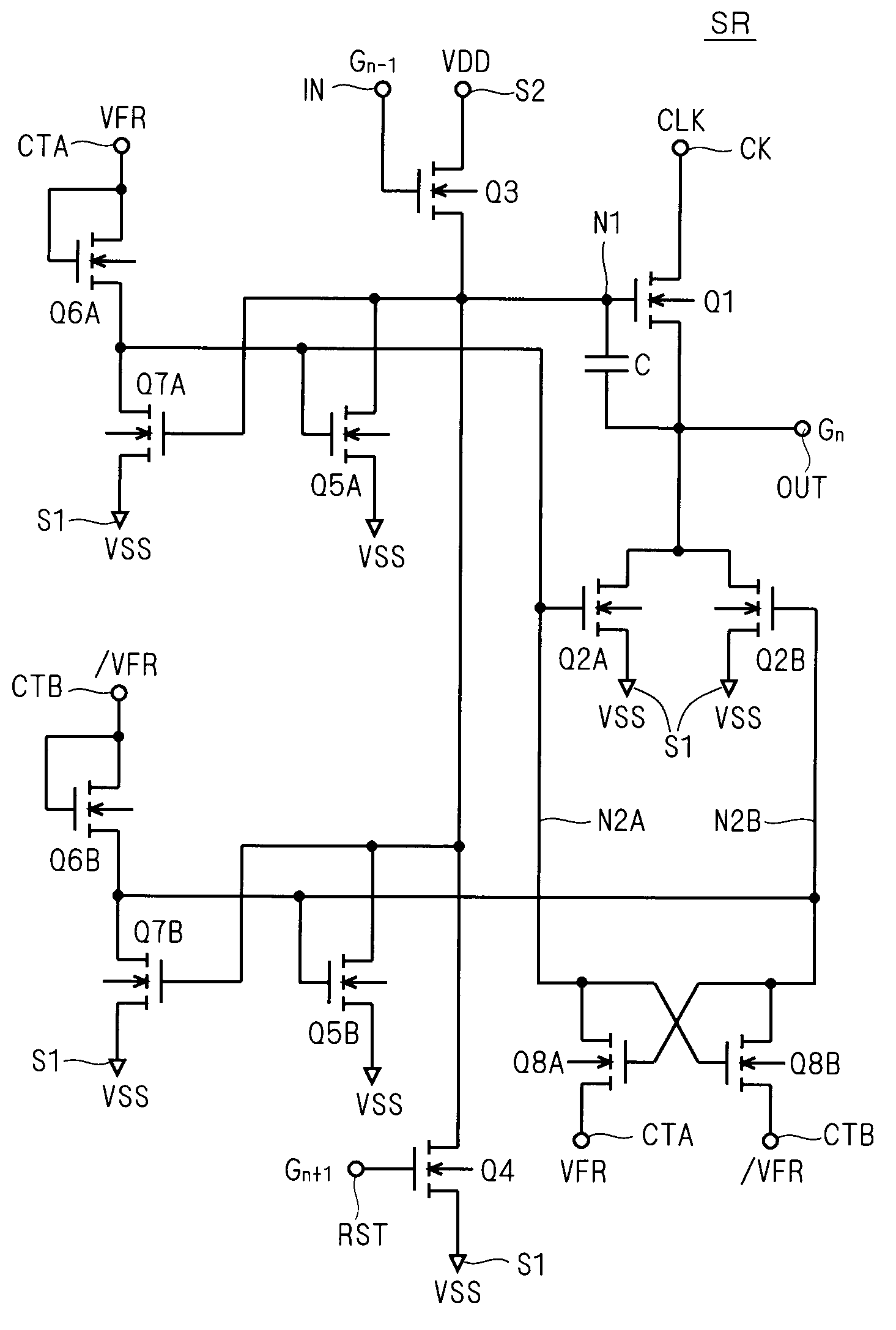
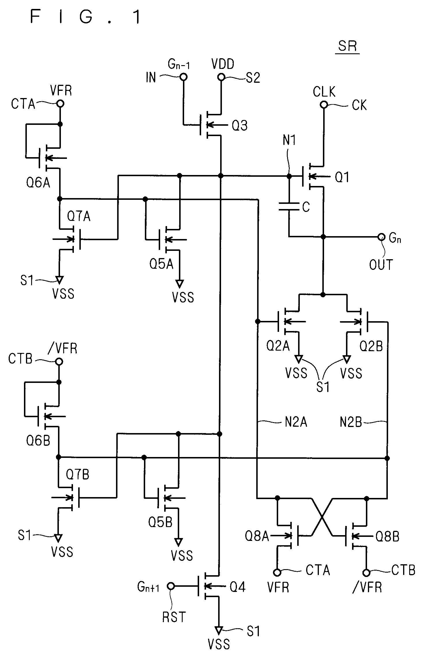
[0047]FIG. 1 is a circuit diagram illustrating the configuration of a unit shift register SR according to a first preferred embodiment of the present invention. The unit shift register SR includes two output pull-down transistors, and alternately activates and deactivates these transistors, to thereby minimize the threshold voltage shift of the output pull-down transistors.

[0048]Transistors constituting the unit shift register SR are all field effect transistors of the same conductivity type, and are all assumed to be N-type TFTs herein. The N-type TFT is in the active (on) state when the gate is at the H level with respect to the source, and in the non-active (off) state at the L level. The unit shift register SR may be formed of P-type transistors. The P-type transistor is in the active (on) state when the gate is at the L level with respect to the source, and in the non-active (off) state at the H level.

[0049]In the following description, it is assumed that a plurality of unit sh...

second preferred embodiment

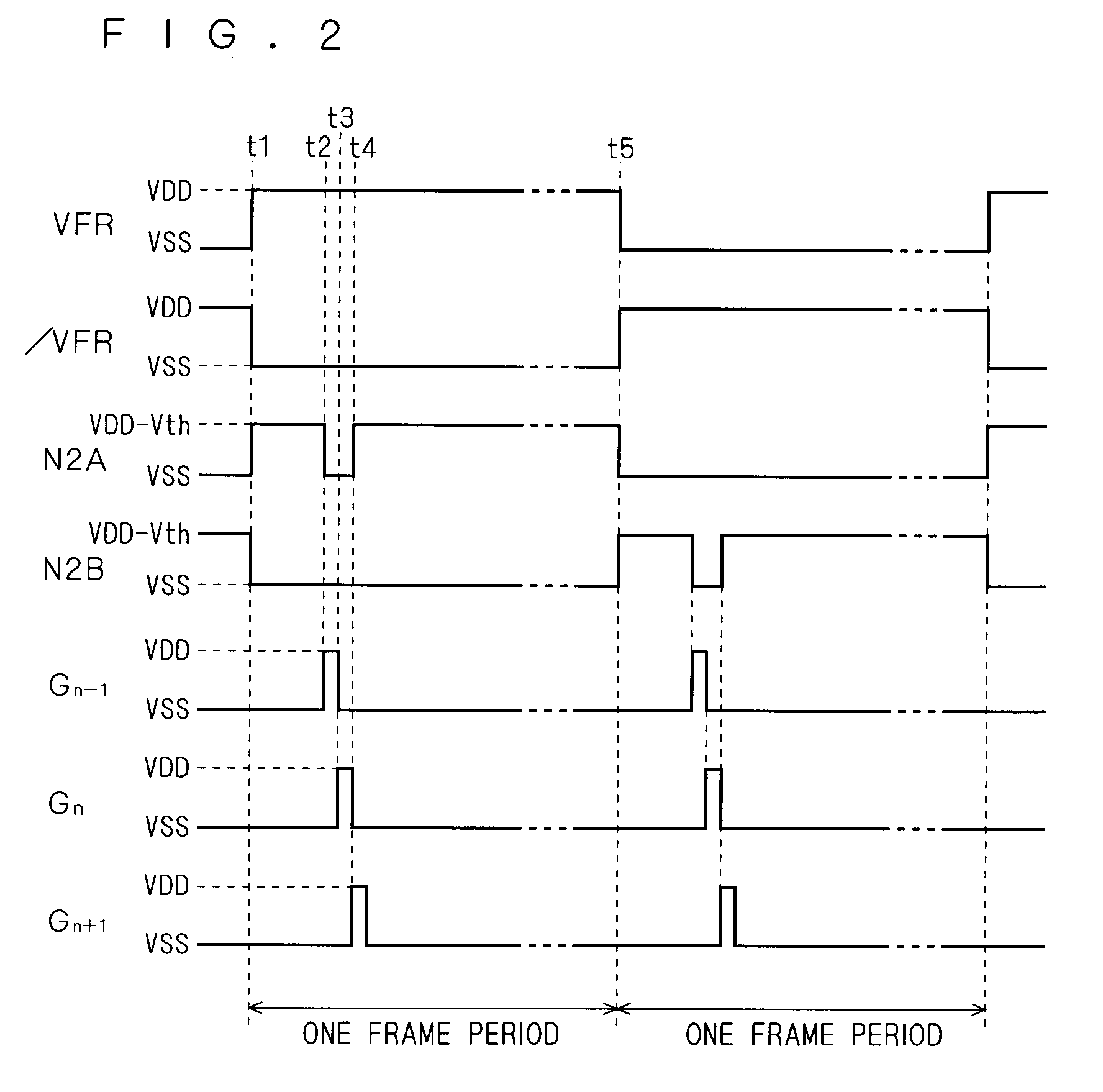
[0101]As described above, the problem of the error signal occurring just after the change in level of the first and second control signals VFR and / VFR results from the low rate of change in level of the nodes N2A and N2B. A second preferred embodiment will therefore present a unit shift register SR in which the nodes N2A and N2B change in level at high speeds just after the change in level of the first and second control signals VFR and / VFR.

[0102]FIG. 6 is a circuit diagram illustrating the configuration of a unit shift register SR according to the second preferred embodiment. The unit shift register SR includes transistors Q13A and Q13B added to the first and second inverters, respectively, in the circuit shown in FIG. 1.

[0103]The transistor Q13A added to the first inverter is connected between the first control terminal CTA supplied with the first control signal VFR and node N2A serving as the output node of the second inverter. The transistor Q13B added to the second inverter i...

third preferred embodiment

[0113]FIG. 8 is a circuit diagram illustrating the configuration of a unit shift register SR according to a third preferred embodiment. The circuit configuration of the unit shift register SR is similar to that of the second preferred embodiment (FIG. 6); in the present embodiment, however, the second reset terminal RST2 receives a start pulse STY as the reset signal NBR. The start pulse STY is a pulse signal corresponding to the head of each frame period of an image signal (i.e., the end of the blanking period), and input to the input terminal IN of the unit shift register SR1 of the forwardmost shift register (of the first stage) as described earlier.

[0114]The start pulse STY corresponds to the head of each frame period, and thus reaches the H level at the end of the blanking period. Therefore, setting the first and second control signals VFR and / VFR to change in level (at time t1, t5) just before the start pulse STY rises to the H level (at time t1S, t5S) as shown in FIG. 9 allo...


PUM


Abstract

A unit shift register includes a first transistor for supplying an output terminal with a clock signal, and second and third transistors for discharging the output terminal, and further includes a fourth transistor having its gate connected to the gate node of the second transistor and discharging the gate node of the first transistor, and a fifth transistor having its gate connected to the gate node of the third transistor and discharging the gate node of the first transistor. Input of the clock signal is prohibited just after the change in level of first and second control signals for switching between the second and third transistors.

Description

BACKGROUND OF THE INVENTION[0001]1. Field of the Invention[0002]The present invention relates to a shift register, and more particularly, to a shift register for use as a scanning-line driving circuit for an image display apparatus or the like, which is formed by field effect transistors of the same conductivity type only.[0003]2. Description of the Background Art[0004]An image display apparatus (hereinafter referred to as a “display apparatus”) such as a liquid crystal display includes a display panel with a plurality of pixels arrayed in a matrix. A gate line (scanning line) is provided for each row of pixels (pixel line) on the display panel, and gate lines are sequentially selected and driven in a cycle of one horizontal period of a display signal, so that a displayed image is updated. As a gate-line driving circuit (scanning-line driving circuit) for sequentially selecting and driving pixel lines, i.e., gate lines, a shift register for performing a shift operation that makes a ...

Claims


Application Information

Patent Timeline
Patent Type & Authority Patents(United States)
IPC IPC(8): G11C19/00
CPCG11C19/28
Inventor TOBITA, YOUICHIMURAI, HIROYUKI
Owner TRIVALE TECH LLC
Why Eureka
Try Eureka