Method and system for manufacturing semiconductor device

a semiconductor and manufacturing technology, applied in the field of method and system for manufacturing semiconductor devices, can solve the problems of unacceptably large electric leakage current, adverse effects on the electric characteristics, native oxides of iii-v semiconductors, etc., and achieve the effects of improving the density of defects at the interface (dit) and the leakage current, and improving the eo

Active Publication Date: 2014-10-14
HONG MING HWEI +7
View PDF8 Cites 0 Cited by
  • Summary
  • Abstract
  • Description
  • Claims
  • Application Information

AI Technical Summary

Benefits of technology

[0006]Since high-quality interfaces between the oxide layer and the semiconductor layer are the key for realizing high performance MOSFETs, a method and system for manufacturing semiconductor devices with the high-quality interfaces by using the in-situ approach are provided, wherein no surface treatments are employed. Based on the method and system provided in the present invention, the electrical properties of the high-κ dielectric film on semiconductors, in particular III-V compound semiconductors, including the capacitance-voltage (C-V) characteristics, the density of defects at the interface (Dit) and the leakage current, and the EOT are all improved.

Problems solved by technology

Beyond this point, electrons tunneling through this insulating layer will give unacceptably large electric leakage currents.
However, when a stacked structure of the high-κ dielectric film and the substrate is formed by using the abovementioned methods, there exists a problem that an interface between the high-κ dielectric film and the substrate is always exposed to the atmosphere, which may cause the generation of the native oxide layer on the substrate, thereby giving adverse effects on the electric characteristics.
The native oxides of III-V semiconductors, unlike SiO2 on Si, are leaky and do not perform high quality native III-V oxides / III-V semiconductors interfaces.
However, the method is not able to completely remove the native oxides.
Moreover, the residual sulfur at oxide / semiconductor interface is thermally unstable and is adverse to the source / drain activation in MOSFET fabrication.

Method used


Image

  • Method and system for manufacturing semiconductor device
  • Method and system for manufacturing semiconductor device
  • Method and system for manufacturing semiconductor device

Examples


first embodiment

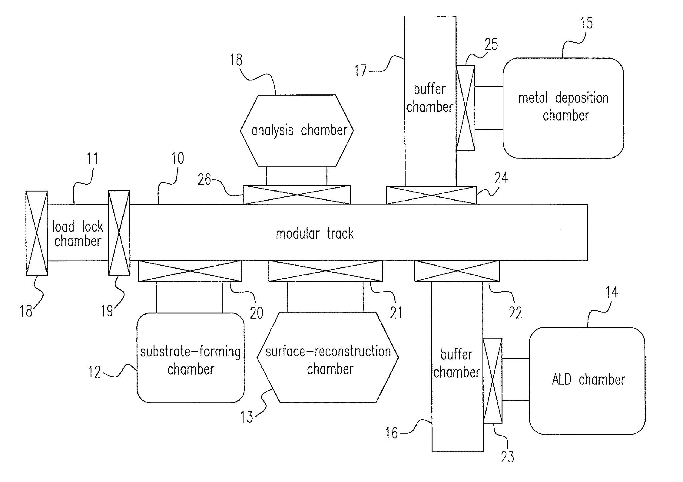
[0022]Please refer to FIG. 1, which is a diagram showing a semiconductor manufacturing system according to the present invention. The system is a multi-chamber system where all chambers are connected with a modular track 10 selectively via valves 18, 19, 20, 21, 22, 23, 24, 25 and 26. In the modular track 10 having a pressure ranged from 10−9 to 10−11 Torr, at least one wafer is transferred into / out of the respective chambers on a wafer stage by at least one wafer transfer arm (not shown). The system mainly includes chambers such as a load lock chamber 11 whose atmospheres are changeable between ultra high vacuum and atmospheric pressure, a substrate-forming chamber 12 for growing a substrate, and an atomic layer deposition (ALD) chamber 14 for depositing a first high-κ dielectric layer on the substrate by the ALD method. The substrate for semiconductor devices could be formed from silicon, compound III-V or II-VI materials, wherein a III-V group compound semiconductor material incl...

second embodiment

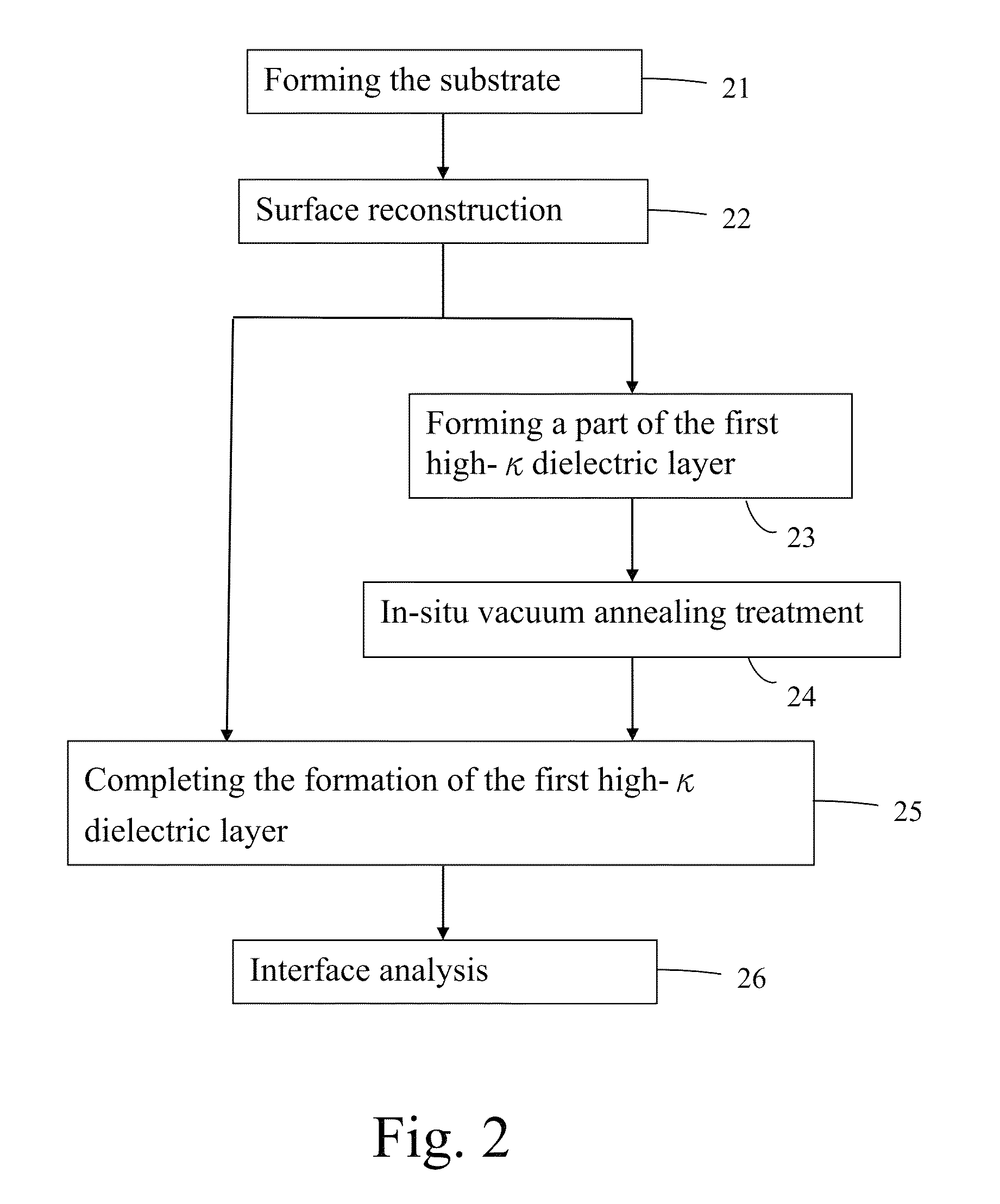
[0027]Alternatively, after Step 22, the samples could be in-situ transferred to the ALD chamber 14 for depositing a part of the first high-κ dielectric layer on the reconstructed surface of the substrate to a first thickness of about 0.15˜1.5 nm (Step 23), and then the samples are in-situ transferred back to the surface-reconstruction chamber 13 so as to perform an in-situ vacuum annealing treatment at a temperature in a range of 300 to 700° C., preferably 450 to 550° C., which is decided by the adopted material of the substrate, and a pressure of 10−7 Torr or less (Step 24). The annealed samples are subsequently in-situ transferred to the ALD chamber 14 for further depositing the rest part of the first high-κ dielectric layer to a desired thickness so as to complete the formation of the first high-κ dielectric layer (Step 25).

[0028]Please refer to FIG. 3, which is a flow chart showing a method for manufacturing a semiconductor device according to a third embodiment of the present ...

third embodiment

[0029]As an example of the third embodiment, an epitaxial compound semiconductor layer (e.g. the p- and n-type In0.53Ga0.47As layer with Be and Si dopants) is grown on single crystal compound semiconductor wafers (e.g. P+ and N+ epi-ready InP(001) wafers) so as to form the substrates (Step 31), and the wafers are in-situ transferred to the surface-reconstruction chamber 13 and heated up to ˜460° C. to obtain (4×2)-reconstructed In / Ga stabilized In0.53Ga0.47As(001) surfaces (Step 32). Then, samples are in-situ transferred to the ALD chamber 14 for the depositions of the second high-κ dielectric layer, i.e. ALD-HfO2 (Step 33), and the first high-κ dielectric layer, i.e. ALD-HfAlO (Step 35) on the formed substrate, wherein the hafnium-based HfAlO with high re-crystallization temperature is employed as the top oxide capping layer to prevent the poly-crystalline formation in the dielectric while providing sufficient high dielectric constant. It is known that HfO2 possesses much higher di...


PUM

PropertyMeasurementUnit
temperatureaaaaaaaaaa
thicknessaaaaaaaaaa
temperatureaaaaaaaaaa

Abstract

The present invention provides a system and method for manufacturing a semiconductor device including a substrate and a high-κ dielectric layer on the substrate. The system comprises a modular track; a substrate-forming chamber connected with the modular track for forming the substrate; and an atomic layer deposition (ALD) chamber connected with the modular track for providing the high-κ dielectric layer.

Description

FIELD OF THE INVENTION[0001]The present invention relates to a method and system for manufacturing semiconductor device, and more particularly to a method and system for manufacturing semiconductor device by using in-situ atomic-layer-deposition method.BACKGROUND OF THE INVENTION[0002]As the downscaling of Si-based MOSFETs, the SiO2 gate oxide thickness is correspondingly reduced to be close to the quantum tunneling limit of 1.0 nm. Beyond this point, electrons tunneling through this insulating layer will give unacceptably large electric leakage currents. HfO2-based high-κ dielectric was introduced to replace SiO2 in 45 nm CMOS technology as the solution to this issue. Moreover, to extend the Moore's Law beyond 15 nm node, it is adamant that III-V high electron mobility semiconductors integrated with high K gate dielectrics has to be employed.[0003]Currently, the chemical vapor deposition (CVD), the atomic layer deposition (ALD), the metal organic chemical vapor deposition (MOCVD), ...

Claims


Application Information

Patent Timeline
Patent Type & Authority Patents(United States)
IPC IPC(8): H01L21/31
CPCH01L21/02194H01L21/022H01L21/28264C23C16/54C23C16/45544H01L21/02178C23C14/568H01L21/0228H01L21/02181H01L29/517
Inventor HONG, MING-HWEIKWO, RAY-NIENPI, TUN-WENHUANG, MAO-LINCHANG, YU-HSINGCHANG, PENLIN, CHUN-ANLIN, TSUNG-DA
Owner HONG MING HWEI
Why Eureka
Try Eureka