Source side self boosting technique for non-volatile memory

a source side and non-volatile memory technology, applied in static storage, digital storage, instruments, etc., can solve the problems of low boosting potential, program disturbance, inadvertent programming, etc., to reduce gidl, minimize program disturbance, and improve self-boosting performance

Inactive Publication Date: 2005-02-22
SANDISK TECH LLC
View PDF27 Cites 801 Cited by
  • Summary
  • Abstract
  • Description
  • Claims
  • Application Information

AI Technical Summary

Benefits of technology

The present invention, roughly described, pertains to technology for programming memory devices in a manner that avoids program disturb. One embodiment includes the programming of a memory system that comprises a set of NAND flash memory strings by increasing the channel potential of the source side of the NAND string in order to improve self boosting performance and minimize program disturb. If the source side neighbor is programmed, then raising the voltage potential of the source side channel of the NAND string reduces GIDL. If the source side neighbor is erased, then raising the voltage potential of the source side channel of the NAND string helps keep the source side neighbor cell from turning on.

Problems solved by technology

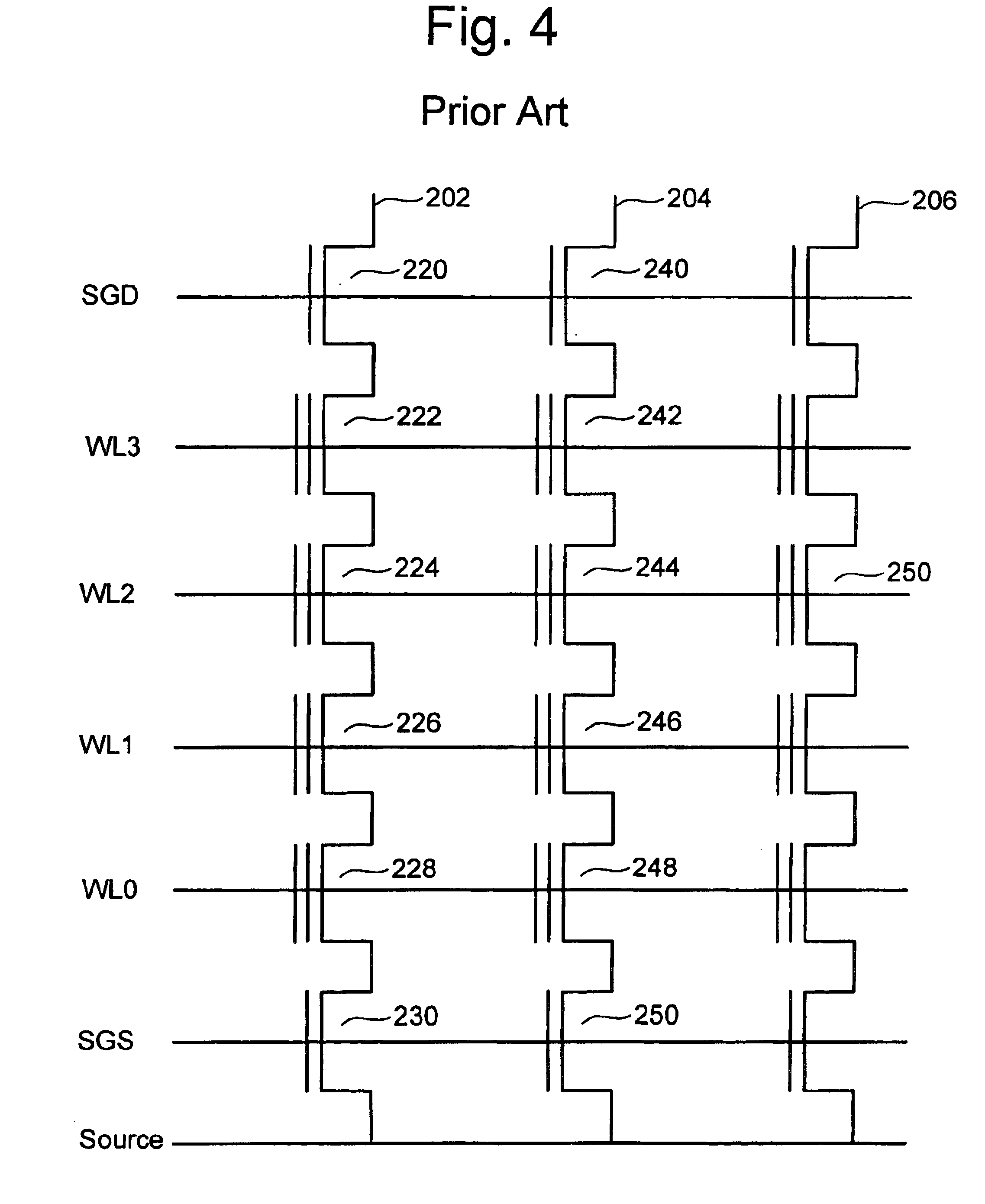
A problem arises when it's desired to program one cell on a word line without programming other cells connected to the same word line, for example, when it's desired to program cell 224 and not cell 244.
Because the program voltage is applied to all cells connected to a word line an unselected cell (a cell that is not to be programmed) on the word line, especially a cell adjacent to the cell selected for programming, may become inadvertently programmed.
Because of this negative charge on the floating gates, the boosting potential doesn't get high enough and there still may be program disturb on the last few word lines.
If Vpass is too low, boosting in the channel is insufficient to prevent program disturb.
While LSB and EASB provide an improvement over self boosting, they also present a problem that depends on whether the source side neighbor cell (cell 246 is the source side neighbor of cell 244) is programmed or erased.
GIDL will cause the boosted voltage to leak away prematurely, resulting in a programming error.
If the leakage current is high enough, the boosting potential in the channel region will go down and there can be program disturb.
Thus, the voltage in the boosted junction will drop quickly, causing program disturb.
Rather that string is operating in self boosting mode, and self boosting mode has the problems discussed above.
This scenario is most likely if other source side cells are programmed, which limits source side boosting.
This issue is most problematic with shorter channel lengths.

Method used


Image

  • Source side self boosting technique for non-volatile memory
  • Source side self boosting technique for non-volatile memory
  • Source side self boosting technique for non-volatile memory

Examples


second embodiment

FIG. 15 depicts a method for programming memory cells according to the present invention. At time t0, the drain voltage (e.g. drain / bit line 442) and drain select control gate (control gate 432) are driven from zero volts to Vdd. The selected word line and the unselected word lines on the drain side are maintained at Vss (e.g. zero volts). The word line for the source side neighbor is kept at Vss; however, the other unselected source side word lines are driven to Vssb. Additionally, the source is driven to Vdd and the control gate of the source side select gate is driven at Vdd (control gate 430). Because the source select gate is turned on, the source is electronically coupled to the string and boosts the voltage potential of source side channel 450. The drain side channel is at a potential of Vdd−Vtd and the source side channel is at a potential of Vdd−Vts, where Vtd is the threshold voltage of the drain side select gate and Vts is the threshold voltage of the source side select g...

third embodiment

FIG. 16 depicts a method for programming memory cells according to the present invention. FIG. 16 uses a similar boosting scheme as illustrated in FIG. 14, with some changes as described below. The drain, drain select, unselected drain side word lines, selected word line, source and source select are the same as in FIG. 14. At time t0 of FIG. 16, the source side channel region is charged to Vdd−Vtd by driving Vssb on all of the source side word lines, as done in FIG. 14. In FIG. 14, the extent of the additional source side boosting is determined by the voltage difference between Vpass and Vssb. However, in FIG. 16 the voltage potential on the source side word lines is reduced to 0v at time ti (where ti is after t0 and before t1). The source side word lines (except the source side neighbor) are then ramped to Vpass at time t1. Initially, as the voltage on the source side control gates is decreasing from Vssb to 0V, the source side channel region will remain at Vdd−Vtd as long as the ...

fourth embodiment

FIG. 17 depicts a method for programming memory cells according to the present invention. FIG. 17 uses a similar boosting scheme as illustrated in FIG. 14; however, the drain select is driven at Vdd+Vtd from t0 to t1 rather than driving the drain select at Vdd. After t1, the drain select is driven at Vdd. Thus, after t1 the drain side channel and the source side channel are at Vdd+Vboost, rather than at Vdd−Vtd+Vboost. In some embodiments, it is easier to increase the drain select rather than the drain. During programming, many bit lines must be selected and the capacitance is large. Only one drain select (or a small number of drain selects) need be selected, thus, the capacitance is relatively small. The timing diagram of FIG. 16 can also be modified as per the teaching of FIG. 17 so that the drain select is driven at Vdd+Vtd rather than driving the drain select at Vdd.


PUM


Abstract

A non-volatile semiconductor memory system (or other type of memory system) is programmed in a manner that avoids program disturb. In one embodiment that includes a flash memory system using a NAND architecture, program disturb is avoided by increasing the channel potential of the source side of the NAND string during the programming process. One exemplar implementation includes applying a voltage (e.g. Vdd) to the source contact and turning on the source side select transistor for the NAND sting corresponding to the cell being inhibited. Another implementation includes applying a pre-charging voltage to the unselected word lines of the NAND string corresponding to the cell being inhibited prior to applying the program voltage.

Description

BACKGROUND OF THE INVENTION1. Field of the InventionThe present invention relates generally to technology for programming memory devices. In one embodiment, the present invention is directed to the programming of a non-volatile memory (e.g. a flash memory device) using a self boosting technique.2. Description of the Related ArtSemiconductor memory devices have become more popular for use in various electronic devices. For example, non-volatile semiconductor memory is used in cellular telephones, digital cameras, personal digital assistants, mobile computing devices, non-mobile computing devices and other devices. Electrical Erasable Programmable Read Only Memory (EEPROM) and flash memory are among the most popular non-volatile semiconductor memories.One example of a flash memory system uses the NAND structure, which includes arranging multiple transistors in series, sandwiched between two select gates. The transistors in series and the select gates are referred to as a NAND string. ...

Claims


Application Information

Patent Timeline
Patent Type & Authority Patents(United States)
IPC IPC(8): G11C16/10G11C16/34G11C11/34G11C16/04G11C16/06G11C11/56
CPCG11C16/3418G11C16/10G11C11/5628G11C16/0483G11C16/3454G11C16/12G11C16/30G11C16/3459
Inventor LUTZE, JEFFREY W.CHEN, JIANLI, YANHIGASHITANI, MASAAKI
Owner SANDISK TECH LLC
Why Eureka
Try Eureka