Semiconductor substrate, semiconductor device, and manufacturing methods of the same

a semiconductor and substrate technology, applied in the direction of polycrystalline material growth, crystal growth process, chemically reactive gas, etc., can solve the problems of reducing the resistivity of silicon carbide substrate, suppressing defects originating from junction interfaces, and reducing manufacturing costs

Pending Publication Date: 2022-05-19
ROHM CO LTD
View PDF0 Cites 0 Cited by
  • Summary
  • Abstract
  • Description
  • Claims
  • Application Information

AI Technical Summary

Benefits of technology

[0071]According to the present disclosure, a room-temperature junction and a diffused junction are not required, and therefore polishing to ensure the surface roughness is not required, and the manufacturing cost is reduced. In addition, since there is no junction interface, defects originating from a junction interface are suppressed.
[0072]Further, a semiconductor substrate which includes an n-type SiC semiconductor layer laminated on a p-type SiC semiconductor layer and is applicable to an IGBT may include an n-type SiC semiconductor layer having high crystallinity. Further, this kind of semiconductor substrate may have ensured throughput a...

Problems solved by technology

However, if a silicon carbide substrate is used for manufacturing various SiC semicon...

Method used


Image

  • Semiconductor substrate, semiconductor device, and manufacturing methods of the same
  • Semiconductor substrate, semiconductor device, and manufacturing methods of the same
  • Semiconductor substrate, semiconductor device, and manufacturing methods of the same

Examples


first embodiment

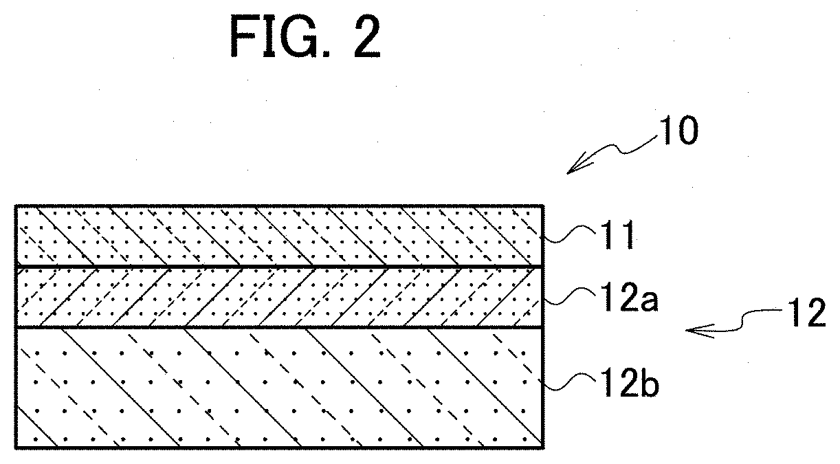
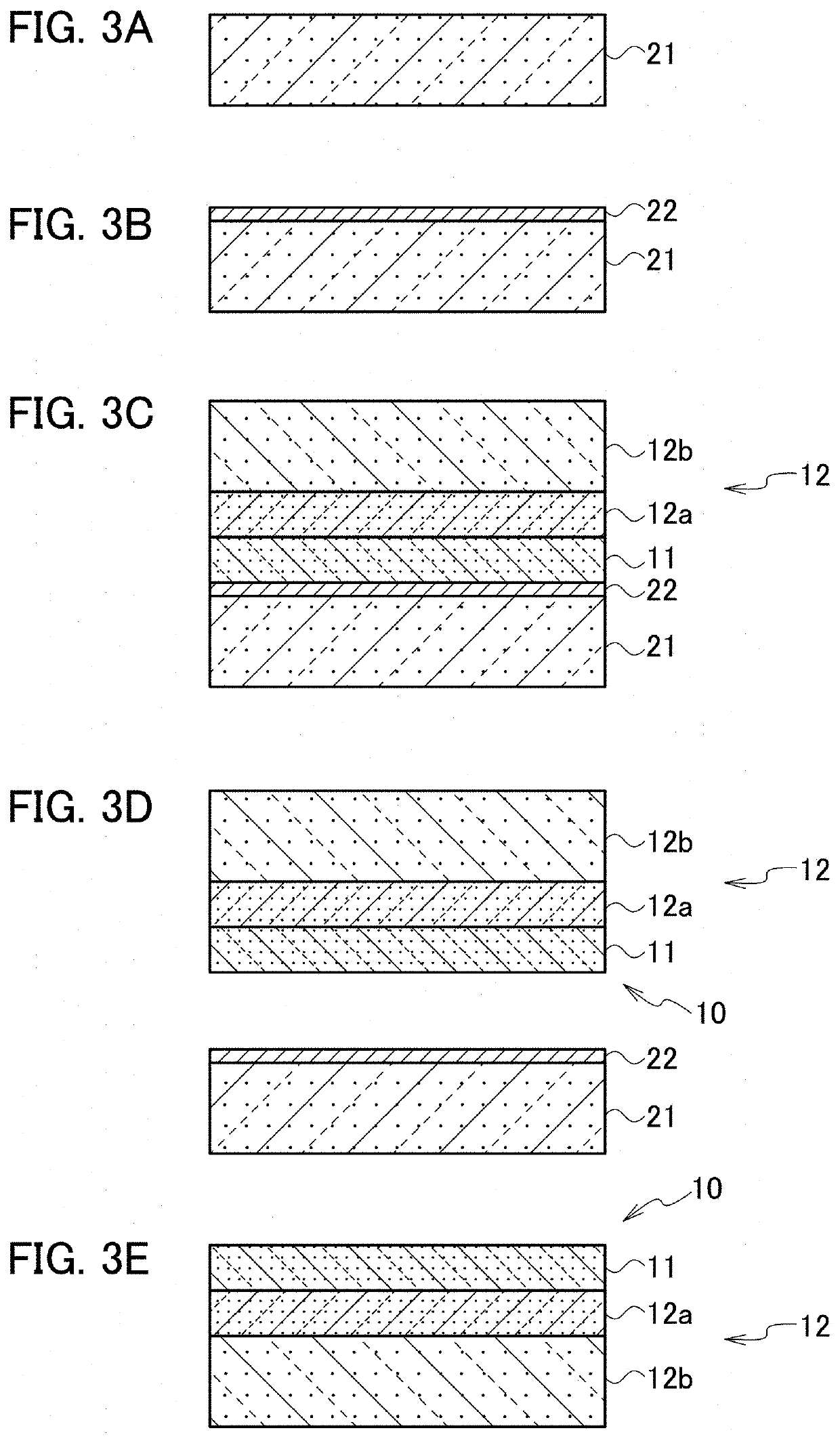
[0120]A semiconductor substrate, a semiconductor device, and manufacturing methods of the same of a first embodiment will be described in detail with reference to the drawings. FIG. 2 is a cross sectional view showing a schematic configuration of a semiconductor substrate of the first embodiment.

[0121]A semiconductor substrate 10 of the first embodiment includes a drift layer 11 of a first layer which is a single crystal SiC semiconductor layer. The semiconductor substrate 10 also includes a buffer layer 12a and a substrate layer 12b of a second layer 12 which is a single crystal or polycrystal SiC semiconductor layer. The buffer layer 12a of the second layer 12 is formed from the surface of the drift layer 11 to a predetermined height in the direction of the second layer 12. The remainder of the second layer 12 on buffer layer 12a which is a layer portion formed beyond the predetermined height from the surface of the drift layer 11 forms the substrate layer 12b of the second layer ...

second embodiment

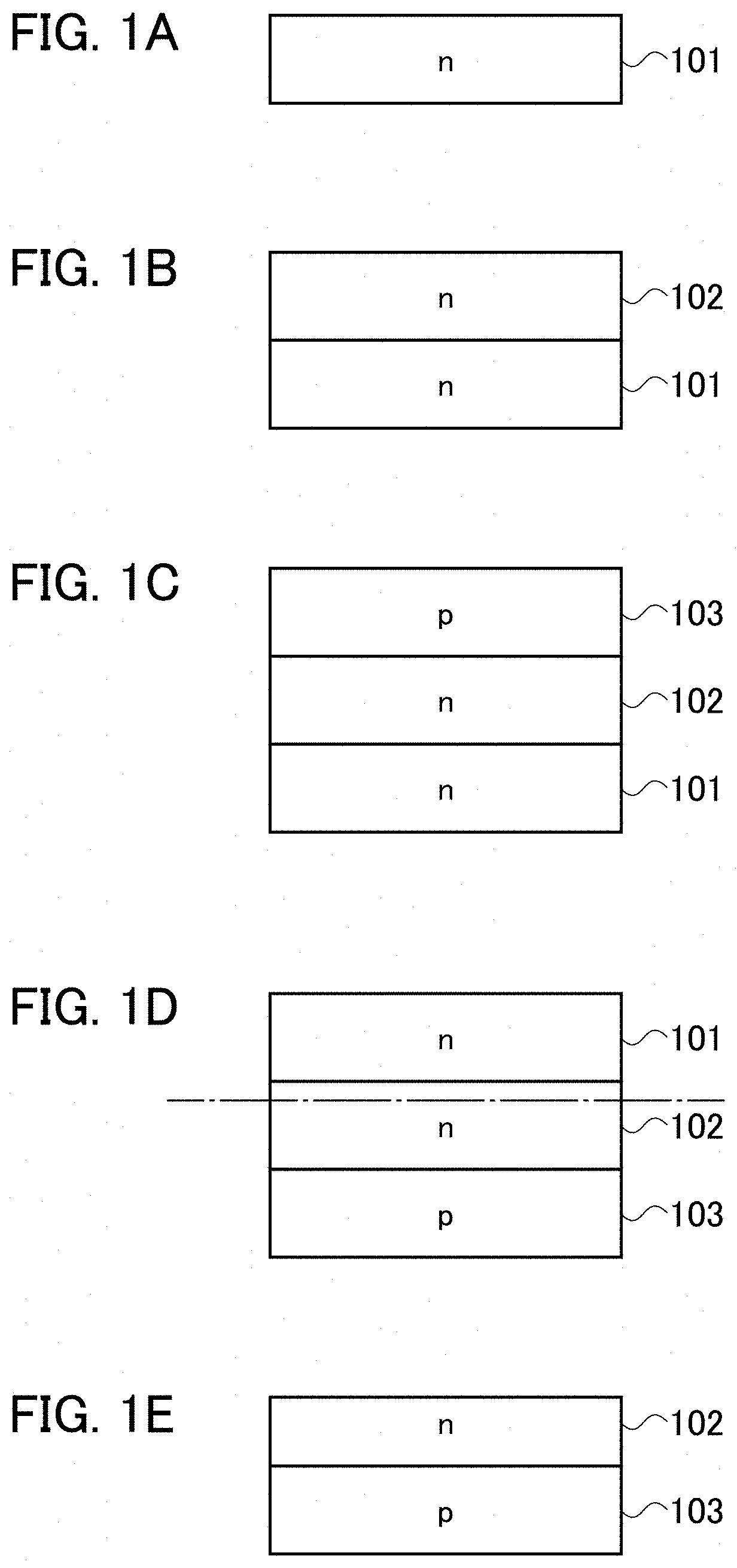
[0157]A semiconductor substrate, a semiconductor device, and manufacturing methods of the same according to a second embodiment will be described. FIGS. 10A to 10C is a flow diagram showing a manufacturing method of a semiconductor substrate of the second embodiment. As shown in FIG. 10A, a p-type SiC semiconductor substrate 211 is provided, and an n-type SiC semiconductor substrate 212 is provided.

[0158]The p-type SiC semiconductor substrate 211 which is a first substrate has a predetermined thickness and one surface as a junction surface. The p-type SiC semiconductor substrate 211 is a p-type SiC semiconductor in which a p-type impurity such as boron or aluminum is doped in SiC, and may be a single crystal or a polycrystal semiconductor substrate. The single crystal p-type SiC semiconductor substrate 211 may be formed based on an epitaxy method in which a single crystal epitaxial layer is grown on a base crystal. Further, a remote epitaxy method may be used in which graphene is fo...

third embodiment

[0192]Next, a third embodiment will be described. In the drawings described below, the same or similar portions are denoted by the same or similar reference numerals. It should be noted, however, that the drawings are schematic and that the relationships between the thickness of each component and the plane dimensions are different from those in reality. Therefore, the specific thickness and dimensions should be determined in consideration of the following description. In addition, it is needless to say that the drawings include parts having different dimensional relationships and ratios.

[0193]Further, the third embodiment shown below exemplifies a device or method for embodying a technical concept, and does not specify the material, shape, structure, arrangement, and the like of each component. Various changes may be made to the third embodiment in the scope of claims.

[0194]Polycrystal Silicon Carbide Substrate

[0195]A polycrystal silicon carbide substrate 310 according to a third e...


PUM

PropertyMeasurementUnit
Thicknessaaaaaaaaaa
Thicknessaaaaaaaaaa
Thicknessaaaaaaaaaa

Abstract

A semiconductor substrate includes a drift layer of a first layer formed of a single crystal SiC semiconductor and a buffer layer and a substrate layer of a second layer that is formed of a SiC semiconductor which includes a polycrystalline structure and is formed on the surface of the first layer, in which the second layer (12) is formed on the surface of the drift layer of the first layer by means of CVD growth, the drift layer of the first layer is formed by means of epitaxial growth, and accordingly, defects occurring at a junction interface of the semiconductor substrate including the single crystal SiC layer and the polycrystal SiC layer are suppressed, and manufacturing costs are also reduced.

Description

CROSS-REFERENCE TO RELATED APPLICATION[0001]This disclosure is a continuation application of International Application No. PCT / JP2020 / 029516, filed on Jul. 31, 2020, which claims the priority of Japanese Patent Application Nos. 2019-142403, 2019-142405, 2019-142409 and 2019-142410, filed on Aug. 1, 2019, the entire contents of which are incorporated by reference herein.TECHNICAL FIELD[0002]The present disclosure relates to a semiconductor substrate and a semiconductor device using SiC, and manufacturing methods of the same. The present disclosure also relates to a polycrystal silicon carbide substrate, a polycrystal silicon carbide ingot, a manufacturing method of a polycrystal silicon carbide substrate, a semiconductor substrate structure, and a power semiconductor device.BACKGROUND ART[0003]For power control applications, devices made of Sic have been provided in the past. Examples of such devices include a Schottky barrier diode (SBD), a MOSFET, and an IGBT (insulated gate bipola...

Claims


Application Information

Patent Timeline
IPC IPC(8): H01L29/16H01L29/04H01L21/02
CPCH01L29/1608H01L29/045H01L21/02378H01L29/7813H01L21/02516H01L21/02595H01L21/02529H01L21/02433C30B25/20C30B29/36H01L21/02598H01L21/02H01L29/78H01L21/0262H01L29/872H01L21/02609H01L21/02664H01L29/04H01L21/0445H01L29/45C04B35/565C23C16/30C23C16/42H01L21/02447H01L21/02513H01L21/02444H01L21/02505H01L29/7395H01L29/7397H01L29/1095H01L29/0623H01L29/66068H01L29/7802C30B30/00
Inventor MAEKAWA, TAKUJIMORIMOTO, MITSURU
Owner ROHM CO LTD
Why Eureka
Try Eureka