Bonding material, electronic component and bonded structure

a technology of electronic components and bonding materials, applied in the field of bonding materials, can solve problems such as lead melting from waste containing solder materials into soil, and achieve the effect of suppressing defects in electronic components and a bonded structure including the sam

Inactive Publication Date: 2010-11-25
PANASONIC CORP
View PDF5 Cites 7 Cited by
  • Summary
  • Abstract
  • Description
  • Claims
  • Application Information

AI Technical Summary

Benefits of technology

[0015]According to the present invention, it is possible to provide a bonding material having a melting temperature of 275° C. or higher and containing no lead. When the bonding material of the present invention is used for internal bonding of an electronic componen

Problems solved by technology

While recent years have seen growing interest in global environmental protection, th

Method used


Image

  • Bonding material, electronic component and bonded structure
  • Bonding material, electronic component and bonded structure
  • Bonding material, electronic component and bonded structure

Examples


embodiment 1

[0026]The bonding material of the present embodiment contains 2 to 10.5% by weight of Cu, 0.02 to 0.2% by weight of Ge, and 89.3 to 97.98% by weight of Bi. The Cu content is preferably 2 to 6% by weight, and the Ge content is preferably 0.05 to 0.1% by weight.

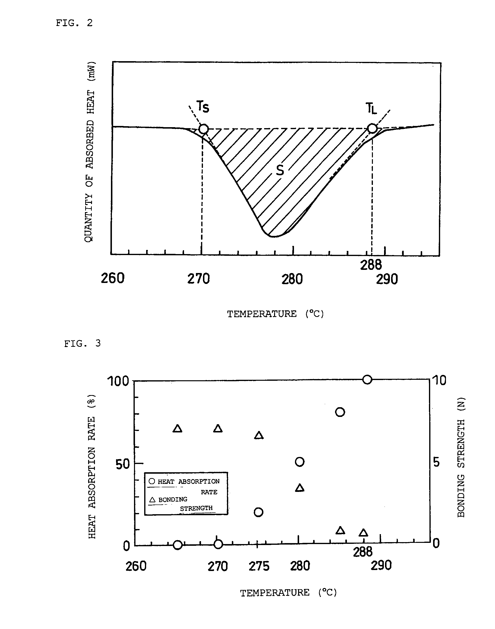
[0027]The bonding material of the present embodiment has heat resistance of up to 275° C., and therefore is suitable as, for example, a bonding material for bonding an electronic element and an electrode within an electronic component such as a power transistor. High heat resistance of the bonding material used in the electronic component suppresses defects in the electronic component that might be caused when bonding the electronic component to a board using a flow soldering machine. Also, the bonding material of the present embodiment contains no lead, which makes it possible to provide lead-free electric or electronic equipment.

[0028]To ensure heat resistance of up to 275° C., it is effective to use a binary alloy (an alloy ...

embodiment 2

[0051]The bonding material of the present embodiment contains 2 to 10.5% by weight of Cu, 0.02 to 0.2% by weight of Ge, 0.02 to 0.11% by weight of Ni, and 89.19 to 97.96% by weight of Bi. The Cu content is preferably 2 to 6% by weight, the Ge content is preferably 0.05 to 0.1% by weight, and the Ni content is preferably 0.05 to 0.08% by weight.

[0052]The bonding material of the present embodiment has higher impact resistance than the bonding material of Embodiment 1.

[0053]The impact resistance can be evaluated by a test in which a 60 g weight is dropped from the height of 180 mm to hit a side surface of a chip capacitor of a 1.6 mm×0.8 mm size.

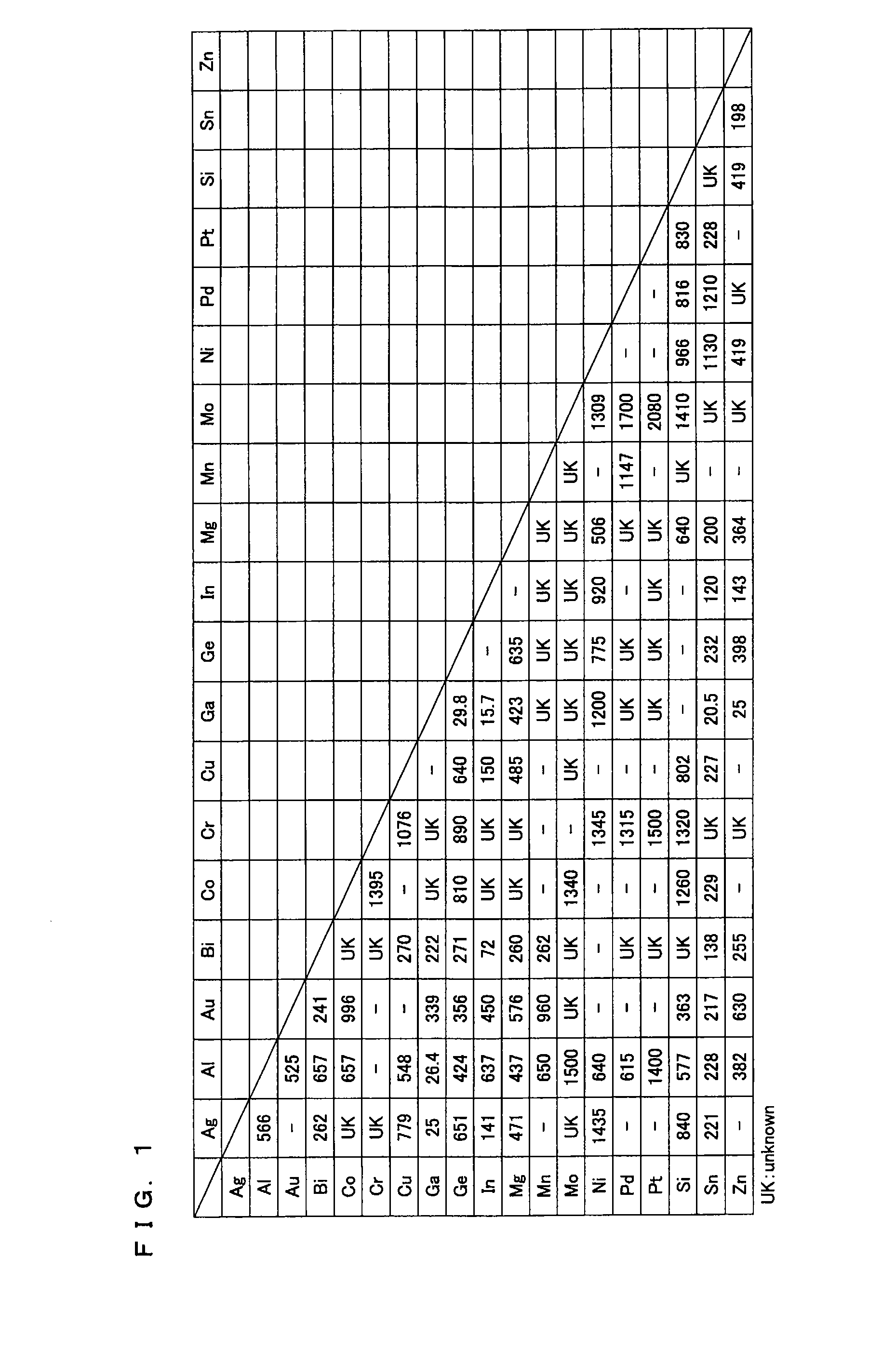
[0054]A chip capacitor having a portion bonded with 92.56 wt % Bi-7.4 wt % Cu-0.04 wt % Ge was subjected to the aforementioned impact resistance test, and broken at the bonded portion. Cross-sectional observation of the broken bonded portion found that the breakage occurred at the interface between α phase abundant in Bi content and β phase abu...

embodiment 3

[0065]The electronic component of the present embodiment includes an electronic element, an electrode connected to the electronic element, and a bonding material for bonding the electronic element and the electrode. Here, as the above bonding material, the bonding material of Embodiment 1 or 2 can be used.

[0066]The electronic element is formed by, but not specifically limited to, for example, an Si chip, an SiC chip, or a coil. The electronic component is not limited to a power transistor, and examples thereof include a chip component, surface-mounted components, such as QFP (Quad Flat Package) and BGA (Ball Grid Array), and insertion components, such as axial components and radial components.

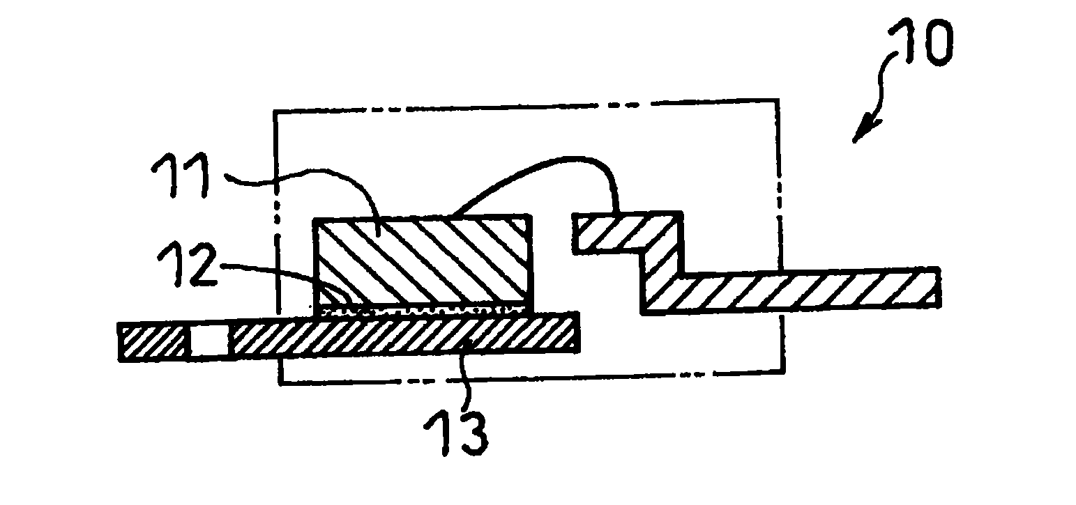
[0067]FIG. 8 is a schematic cross-sectional view illustrating the structure of a power transistor as an example of the electronic component of the present embodiment. The power transistor 10 is a semiconductor mounting component which is loaded with high voltage or current to generate intense h...


PUM

PropertyMeasurementUnit
Temperatureaaaaaaaaaa
Percent by massaaaaaaaaaa

Abstract

A bonding material containing 2 to 10.5% by weight of Cu, 0.02 to 0.2% by weight of Ge and 89.3 to 97.98% by weight of Bi has heat resistance of up to 275° C. and superior wettability, and a bonding material containing 2 to 10.5% by weight of Cu, 0.02 to 0.2% by weight of Ge, 0.02 to 0.11% by weight of Ni and 89.19 to 97.96% by weight of Bi has more superior heat resistance.

Description

TECHNICAL FIELD[0001]The present invention relates to bonding materials (solder materials) containing no lead, as well as electronic components and bonded structures using such a bonding material, particularly to a bonding material for connecting an electronic element and an electrode that make up an electronic component, and more particularly to a bonding material which does not melt due to heating for bonding an electronic component to a board.BACKGROUND ART[0002]While recent years have seen growing interest in global environmental protection, there are concerns about lead melting from waste containing solder materials into soil. Accordingly, to address environmental issues, “lead-free” solder materials containing no lead have been developed, and in particular, high heat-resistant lead-free solder materials are attracting attention.[0003]A typical application using the high heat-resistant lead-free solder material is internal bonding of an electronic component such as a power tran...

Claims


Application Information

Patent Timeline
IPC IPC(8): H05K1/02C22C12/00
CPCB23K35/264B23K2201/36C22C12/00H01L23/49513H01L24/29H01L24/45H01L24/48H01L24/83H01L2224/29113H01L2224/32245H01L2224/45144H01L2224/48091H01L2224/48247H01L2224/73265H01L2224/838H01L2924/01002H01L2924/01003H01L2924/01004H01L2924/01013H01L2924/01014H01L2924/01029H01L2924/01032H01L2924/01033H01L2924/01047H01L2924/0105H01L2924/01051H01L2924/01079H01L2924/01082H01L2924/01322H01L2924/10253H01L2924/10272H01L2924/19041H01L2924/0132H01L2224/2919H01L2924/01005H01L2924/01006H01L2924/01074H01L2924/014H01L2924/0665H01L2224/29101H01L2924/0133H01L2924/0134H01L2924/0001H01L2924/15747H01L2224/29111H01L2924/01028H01L2924/00014H01L2924/00H01L2924/01083H01L2924/3512H01L2224/29099H01L2924/181B23K2101/36H01L2924/00012
Inventor FURUSAWA, AKIOSAKAGUCHI, SHIGEKISUETSUGU, KENICHIRO
Owner PANASONIC CORP
Why Eureka
Try Eureka