Semiconductor laser device and method for fabricating the same

a semiconductor laser and laser device technology, applied in semiconductor lasers, laser details, nanotechnology, etc., can solve the problems of difficult to achieve high output, and known nitride semiconductor laser devices, etc., to achieve high output operation, reduce waveguide loss, suppress the effect of operation current increas

Inactive Publication Date: 2005-12-22
PANASONIC CORP
View PDF2 Cites 57 Cited by
  • Summary
  • Abstract
  • Description
  • Claims
  • Application Information

AI Technical Summary

Benefits of technology

[0022] In the inventive semiconductor laser device, it is preferable that, when as the plurality of dielectric films, three layers are formed, a total thickness of the first dielectric film, the second dielectric film and the third dielectric film is 20 nm or more and 200 nm or less. Thus, it is possible to reduce waveguide loss and suppress increase in operation current in a high output operation. Moreover, the thicknesses of the plurality of dielectric films are relatively small, so that the thickness of the dielectric films in part of the substrate located at the side of the ridge portion is reduced. Therefore, liftoff can be performed in a simple manner.
[0023] It is preferable that the inventive semiconductor l

Problems solved by technology

The present inventor has conducted various examinations for the known nitride semiconductor laser device described above and, as a result, found that the known nitride semiconductor laser device has the following problems.
First, in the known nitride semiconductor laser device, it is difficult to achieve a high output characteristic which allows an output of 65 mW or more in required pulse oscillation or an output of 30 mW or more in continuous wave oscillation.
Accordingly, due to reducti

Method used


Image

  • Semiconductor laser device and method for fabricating the same
  • Semiconductor laser device and method for fabricating the same
  • Semiconductor laser device and method for fabricating the same

Examples


first embodiment

Modified Example of First Embodiment

[0098] Hereinafter, a modified example of the first embodiment of the present invention will be described with reference to the accompanying drawings.

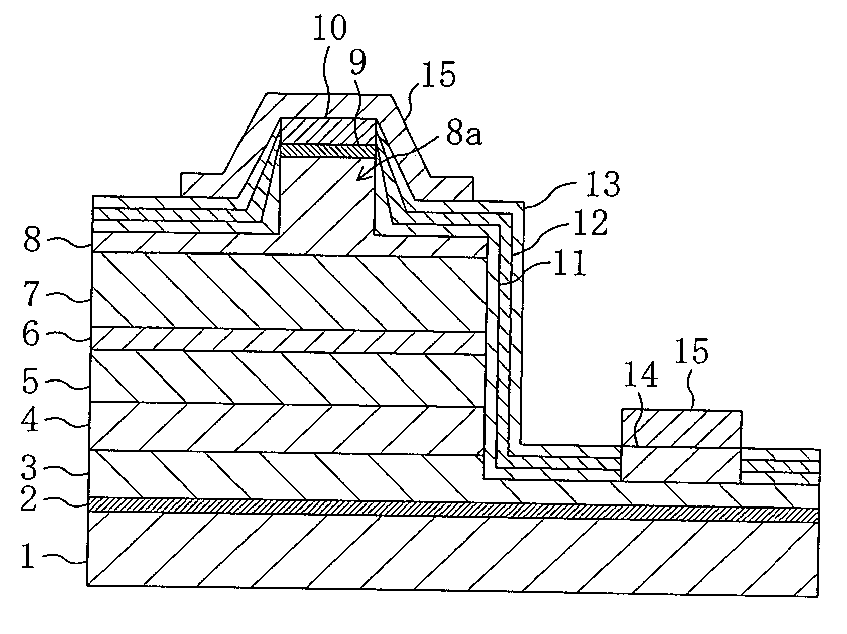
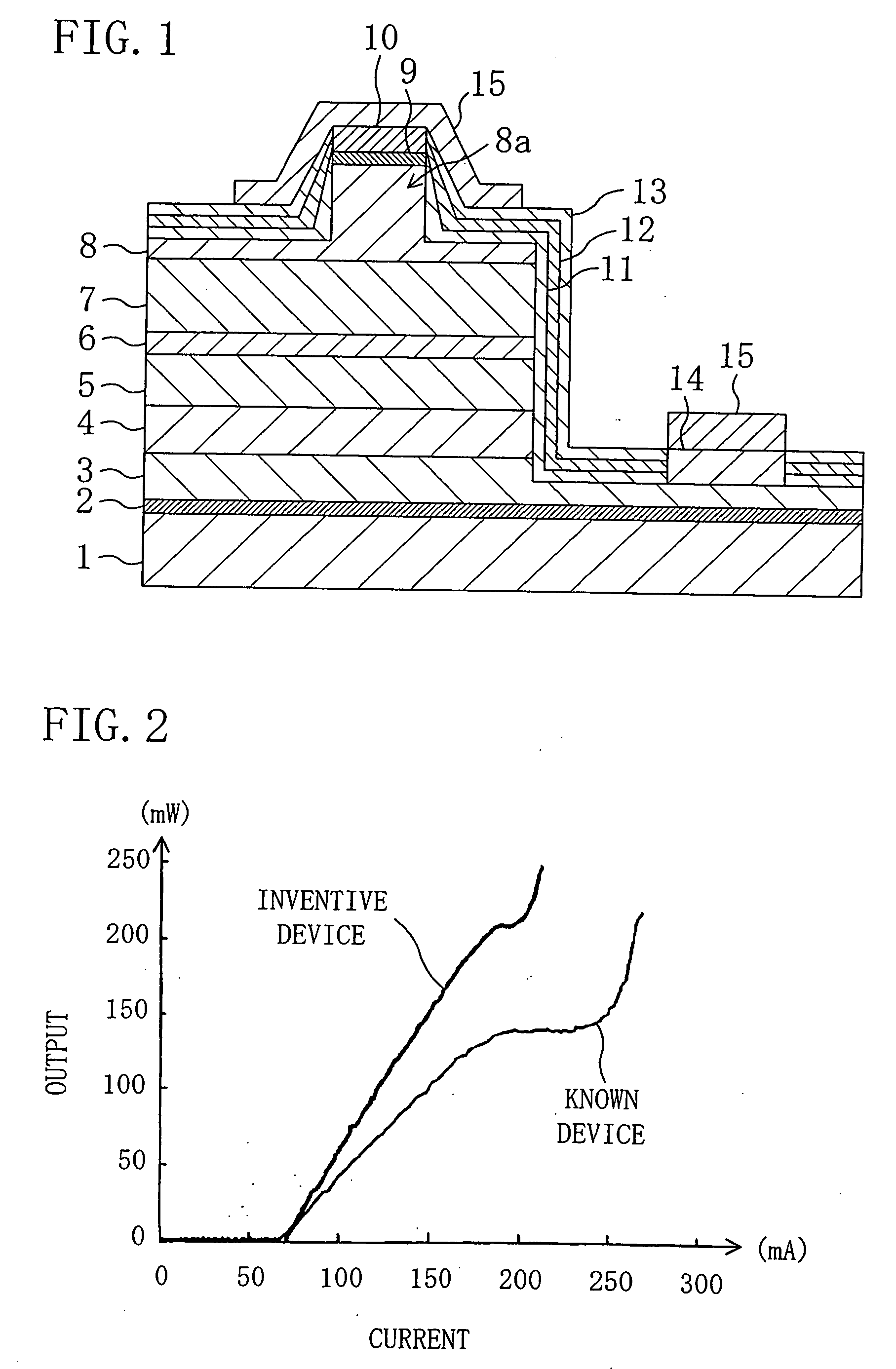
[0099]FIG. 11 is a cross-sectional view illustrating a GaN-based semiconductor laser device according to a modified example of the first embodiment of the present invention. In FIG. 11, each member also shown in FIG. 1 is identified by the same reference numeral and therefore the description thereof will be omitted.

[0100] As shown in FIG. 11, in the semiconductor laser device of this modified embodiment, the n-side electrode 14 is formed not on the n-type contact layer 3 of n-type GaN but on a surface (i.e., backside surface) of the substrate 1 located on a different side from a side on which the lower temperature growth buffer layer 2 of n-type GaN is formed, instead.

[0101] Thus, the step of etching the n-type contact layer 3 and the step of forming an opening for n-side electrode formation in ea...

second embodiment

[0103] Hereinafter, a second embodiment of the present invention will be described with reference to the accompanying drawings.

[0104]FIG. 12 is a cross-sectional view illustrating a GaN-based semiconductor laser device according to the second embodiment of the present invention. In FIG. 12, each member also shown in FIG. 1 is identified by the same reference numeral and therefore the description thereof will be omitted.

[0105] The semiconductor laser device of the second embodiment differs from that of the first embodiment in that a p-side electrode is formed in a different method. Specifically, in the first embodiment, the p-side electrode 10 in which the first metal lamination film for electrode and the second metal lamination film for liftoff are formed in advance is formed. In the second embodiment, however, a metal lamination film for liftoff is formed first, a dielectric film made of three layers is lifted off, and then a metal lamination film for p-side electrode formation i...

third embodiment

[0126] Hereinafter, a third embodiment of the present invention will be described with reference to the accompanying drawings.

[0127]FIG. 15 is a cross-sectional view illustrating a GaN-based semiconductor layer device according to the third embodiment of the present invention. In FIG. 15, each member also shown in FIG. 1 is identified by the same reference numeral and therefore the description thereof will be omitted.

[0128] The semiconductor laser device of the third embodiment differs from the semiconductor laser device of the first embodiment in that a dielectric lamination film covering part of the substrate located outside of the ridge portion 8a is formed so as to have a two-layer structure including the first dielectric film 11 and the second dielectric film 12.

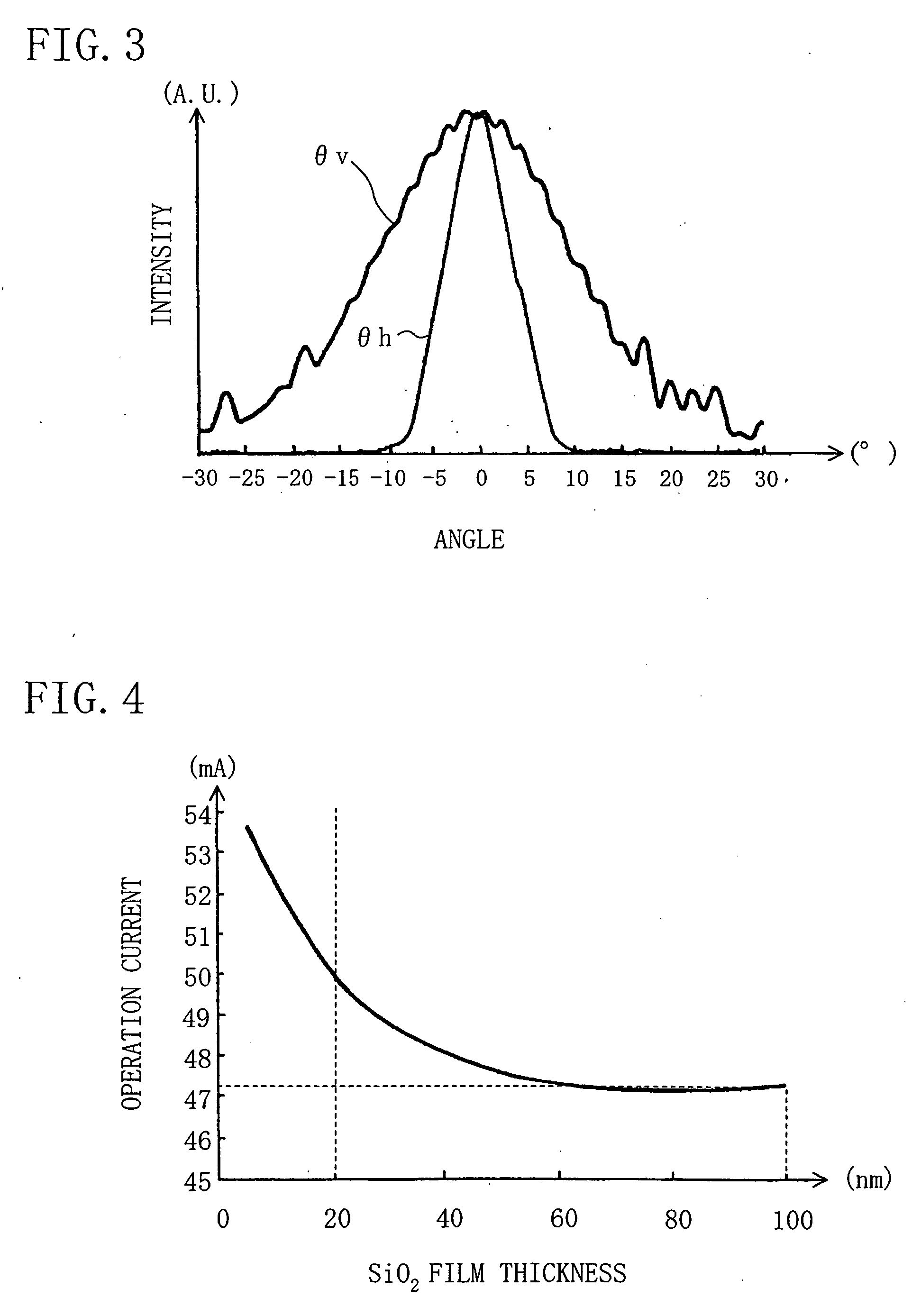
[0129] In the third embodiment, to make waveguide loss as small as possible, it is necessary to use a material having a small absorption for an oscillation wavelength and to trap light in a waveguide. To achieve this...


PUM


Abstract

A semiconductor laser device includes a MQW active layer, a p-type cladding layer formed on the MQW active layer, having a ridge portion and having a smaller refractive index than that of the MQW active layer, a plurality of dielectric films formed at least on part of the p-type cladding layer extending from each side of the ridge portion.

Description

CROSS-REFERENCE TO RELATED APPLICATION [0001] The disclosure of Japanese Patent Application No. 2004-72579 filed on Mar. 15, 2004 including specification, drawings and claims are incorporated herein by reference in its entirety. BACKGROUND OF THE INVENTION [0002] The present invention relates to a semiconductor laser device and a method for fabricating the semiconductor laser device, and more particularly relates to a semiconductor laser device for an optical pickup light source used in an optical information processing device such as an optical disk system and a method for fabricating the semiconductor laser device. [0003] As a light source for a next generation high-density optical disk, there is a strong demand for a laser light source in the blue-violet region, which emits light in the short wave region (i.e., the 400 nm region) which allows reduction in a focusing spot diameter on an optical disk, compared to light in the red region and the infrared region, and is effective in ...

Claims


Application Information

Patent Timeline
IPC IPC(8): H01S5/00H01S5/042H01S5/22H01S5/223H01S5/343
CPCB82Y20/00H01S5/0425H01S5/2214H01S5/222H01S2304/04H01S5/2231H01S5/34333H01S2301/185H01S5/2224H01S5/04252H01S5/04257
Inventor MOCHIDA, ATSUNORI
Owner PANASONIC CORP
Why Eureka
Try Eureka