Nitride-based light-emitting device

a light-emitting device and nitride-based technology, applied in semiconductor devices, light-emitting devices, semiconductor lasers, etc., can solve problems such as insufficientness, and achieve the effects of reducing operating voltage, reducing waveguide loss, and suppressing leakage curren

Active Publication Date: 2020-06-09
PANASONIC SEMICON SOLUTIONS CO LTD
View PDF21 Cites 0 Cited by
  • Summary
  • Abstract
  • Description
  • Claims
  • Application Information

AI Technical Summary

Benefits of technology

[0007]To reduce power consumption in the light-emitting device as much as possible, merely suppressing leakage current is not sufficient, and it is necessary to simultaneously reduce waveguide loss, suppress leakage current, and reduce operating voltage.
[0008]The present disclosure has an object of providing a light-emitting device that can simultaneously reduce waveguide loss, suppress leakage current, and reduce operating voltage.
[0010]According to the present disclosure, a light-emitting device that can simultaneously reduce waveguide loss, suppress leakage current, and reduce operating voltage can be provided.

Problems solved by technology

To reduce power consumption in the light-emitting device as much as possible, merely suppressing leakage current is not sufficient, and it is necessary to simultaneously reduce waveguide loss, suppress leakage current, and reduce operating voltage.

Method used


Image

  • Nitride-based light-emitting device
  • Nitride-based light-emitting device
  • Nitride-based light-emitting device

Examples


embodiment 1

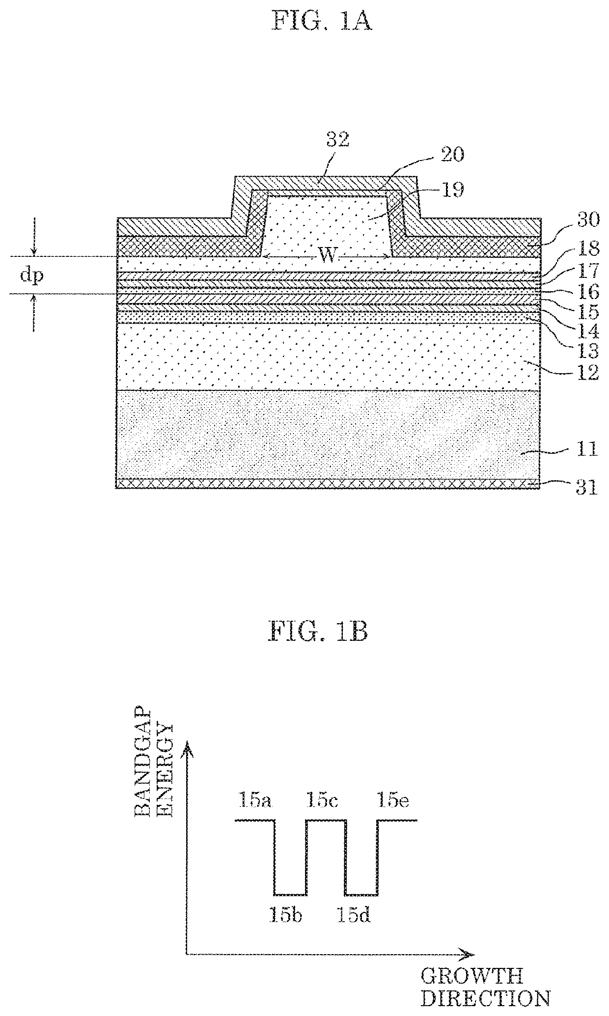
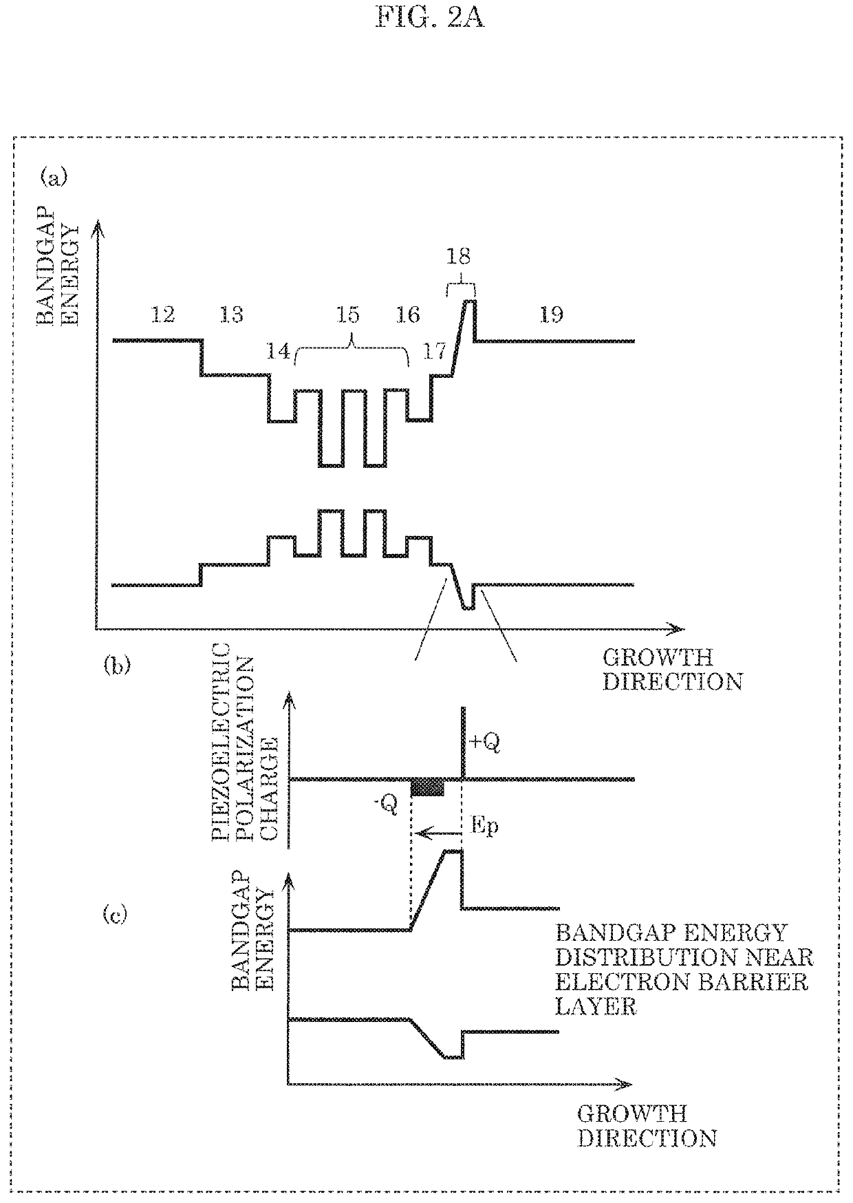
[0065]FIG. 1A illustrates the sectional structure of a nitride-based light-emitting device (hereafter also simply referred to as “light-emitting device”) according to Embodiment 1. FIG. 1A is a sectional view of a light-emitting device including GaN substrate 11, and, on GaN substrate 11: N-type AlGaN cladding layer 12 (film thickness: 1.2 μm); second light guide layer 13 (100 nm) made of N-type GaN; third light guide layer 14 (film thickness: 185 nm) made of undoped InGaN; undoped multiquantum well active layer 15; first light guide layer 16 (film thickness: 100 nm) made of undoped InGaN; intermediate layer 17 (film thickness: 5 nm) made of P-type GaN; P-type electron barrier layer 18; P-type AlGaN cladding layer 19 (film thickness: 660 nm); P-type GaN contact layer 20 (film thickness: 0.1 μm); current block layer 30 transparent to a light distribution; N-type electrode 31; and P-type electrode 32. The width (W) of the ridge is 16.0 μm.

[0066]The distance between the ridge upper por...

embodiment 2

[0170]A light-emitting device according to Embodiment 2 is described below.

[0171]In the light-emitting device according to the foregoing Embodiment 1, the Al composition distribution of electron barrier layer 18 and the Mg doping profile of P-type AlGaN cladding layer 19 and electron barrier layer 18 are designed in detail to achieve all of low voltage, low waveguide loss, and ΔE increase. In the structure of the light-emitting device according to Embodiment 2 of the present disclosure, the doping profile of N-type layers including N-type AlGaN cladding layer 12, second light guide layer 13, and third light guide layer 14 is also adjusted to achieve further loss reduction and voltage reduction. The light-emitting device according to this embodiment is described below.

[0172]An N-type impurity doping profile is described first. In the structure of the light-emitting device according to Embodiment 1, N-type AlGaN cladding layer 12 and second light guide layer 13 are doped with Si of 1×...

embodiment 3

[0193]A light-emitting device according to Embodiment 3 is described below.

[0194]In the structure illustrated in FIG. 15 in Embodiment 2, by setting N1 and N2 to 2×1018 cm−3 or more and 2.5×1018 cm−3 or less and setting high-concentration impurity regions 12a and 13a to be ±5 nm (region width: 10 nm) or more and ±10 nm (region width: 20 nm) or less from the interface between N-type AlGaN cladding layer 12 and second light guide layer 13, a waveguide loss reduction of 0.2 cm−1 or more can be achieved while maintaining the same operating voltage as in the case where N-type AlGaN cladding layer 12 and second light guide layer 13 are uniformly doped with Si of 1×1018 cm−3.

[0195]In Embodiment 3 of the present disclosure, the structure in Embodiment 2 is modified so that N1 and N2 are 2×1018 cm−3 and high-concentration impurity regions 12a and 13a are in a range of ±5 nm (region width: 10 nm) from the interface between N-type AlGaN cladding layer 12 and second light guide layer 13. In thi...


PUM

PropertyMeasurementUnit
distanceaaaaaaaaaa
thicknessaaaaaaaaaa
thicknessaaaaaaaaaa

Abstract

A nitride-based light-emitting device includes, on a GaN substrate: a first-conductivity-side first semiconductor layer; an active layer; and a second-conductivity-side first semiconductor layer, in the stated order, and further includes an electron barrier layer of a second conductivity type between the active layer and the second-conductivity-side first semiconductor layer, the electron barrier layer including a nitride-based semiconductor containing at least Al. The electron barrier layer has a first region in which an Al composition changes. The Al composition in the first region monotonically increases in a direction from the active layer to the second-conductivity-side first semiconductor layer. An impurity concentration in the second-conductivity-side first semiconductor layer is lower in a region nearer the electron barrier layer than in a region farther from the electron barrier layer.

Description

CROSS REFERENCE TO RELATED APPLICATIONS[0001]This application is a U.S. continuation application of PCT International Patent Application Number PCT / JP2017 / 014061 filed on Apr. 4, 2017, claiming the benefit of priority of Japanese Patent Application Number 2016-097459 filed on May 13, 2016, the entire contents of which are hereby incorporated by reference.BACKGROUND1. Technical Field[0002]The present disclosure relates to a nitride-based light-emitting device.2. Description of the Related Art[0003]As light sources for vehicle headlights, halogen lamps, high-intensity discharge (HID) headlamps, and light-emitting diode (LED) lamps are widely used today. HID is currently dominant for headlights, and is used in fog lamps, vehicle dress-up light sources, and the like.[0004]Laser headlight light sources that use, as light-emitting devices higher in light emission intensity than LEDs, laser diodes (LDs) to enhance light emission intensity are attracting attention recently. As a light-emitt...

Claims


Application Information

Patent Timeline
Patent Type & Authority Patents(United States)
IPC IPC(8): H01S5/20H01S5/343H01S5/30H01L33/14H01S5/22H01L33/32F21S41/176F21S41/16F21Y115/30
CPCH01L33/145H01S5/34333H01S5/3054H01S5/2009H01S5/34346F21S41/176F21Y2115/30F21S41/16H01L33/32H01S5/22
Inventor TAKAYAMA, TORUNAKATANI, TOUGOKANO, TAKASHISAMONJI, KATSUYA
Owner PANASONIC SEMICON SOLUTIONS CO LTD
Why Eureka
Try Eureka