Multilayered circuit board and semiconductor device

a multi-layer circuit board and semiconductor technology, applied in the direction of semiconductor/solid-state device details, printed circuit stress/warp reduction, printed circuit aspects, etc., can solve the problems of the above problem, the multi-layer circuit board largely warps in the manufacturing process,

Inactive Publication Date: 2012-07-24
SUMITOMO BAKELITE CO LTD
View PDF11 Cites 60 Cited by
  • Summary
  • Abstract
  • Description
  • Claims
  • Application Information

AI Technical Summary

Benefits of technology

[0056]Furthermore, a Young's modulus of the glass cloth to be used in the present invention is preferably in the range of 62 to 100 GPa, more preferably in the range of 65 to 92 GPa, and even more preferably in the range of 86 to 92 GPa. In the case where the Young's modulus of the glass cloth is a value within the above range, it is possible to effectively suppress deformation of the multilayered circuit board which would occur due to reflow heat during a process of mounting a semiconductor element thereon. This makes it possible to improve connection reliability between the multilayered circuit board and the semiconductor element.

Problems solved by technology

However, since the conductor circuit layers and the insulator layers are single-side laminated together, in the case where conventional insulator layers are used as the insulator layers, there is a problem in that the multilayered circuit board largely warps in a manufacturing process thereof.
However, even in the case where such a method is used, the above problem cannot be sufficiently solved.

Method used


Image

  • Multilayered circuit board and semiconductor device
  • Multilayered circuit board and semiconductor device
  • Multilayered circuit board and semiconductor device

Examples


example 1

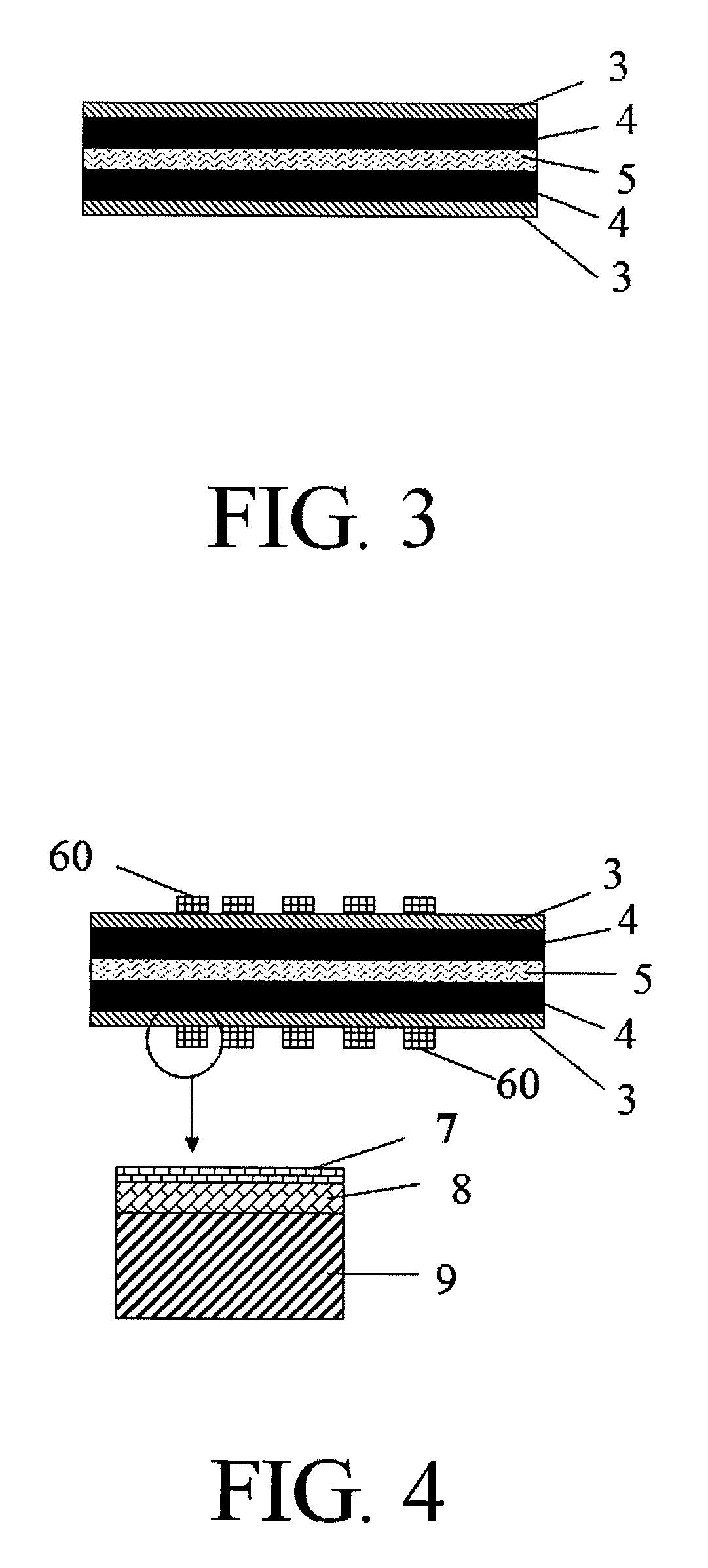
[0070]First, a prepreg 5 having a thickness of 0.2 mm (“EI-6785GS” produced by SUMITOMO BAKELITE Co., Ltd.) was placed between two peelable type copper foils with carrier copper foils each having a size of 250×250 mm square (product name of “F-DP ultra thin electrolytic copper foil with copper carrier” produced by FURUKAWA ELECTRIC Co., Ltd.) so that carrier copper foils 4 of the copper foils with carrier copper foils made contact with the prepreg 5, and then the same was pressed at a pressure of 3 MPa and heated at a temperature of 180° C. for 1 hour to obtain a support base member (see FIG. 3). In this regard, in the copper foil with carrier copper foil, a thickness of the copper foil was 9 μm and a thickness of the carrier copper foil was 70 μm.

[0071]Both surfaces of the support base member were subjected to a soft etching treatment, dry-film resists each having a thickness of 20 μm (“AR-320” produced by TOKYO OHKA KOGYO Co., Ltd.) were laminated to both surfaces of the support b...

example 2

[0082]Basically, multilayered circuit boards each having a single-side laminated structure were manufactured in the same manner as in Example 1 except that insulator layers “b” each having a thickness of 40 μm (“APL-3601” produced by SUMITOMO BAKELITE Co., Ltd.) were used instead of the insulator layers “a”. In this regard, each insulator layer “b” was supported by a PET film which was a support film.

[0083]Hereinbelow, description will be made to points different from Example 1.

[0084]The insulator layer “b” was laminated to the surface of each conductor circuit layer 60 using a vacuum press machine (“MVLP-500 / 600-IIA” produced by MEIKI Co., Ltd.) at a first heating and pressing condition in which a temperature was 80° C. and a pressure was 0.5 MPa and at a second heating and pressing condition in which a temperature was 100° C. and a pressure was 1.0 MPa. Thereafter, the PET films were removed from the insulator layers “b”, and then the insulator layers “b” were heated at a temperat...

example 3

1. Preparation of Resin Composition Varnish

[0088]15 parts by weight of novolak type cyanate resin having a weight average molecular weight of about 2,600 (“Primaset PT-30” produced by LONZA Japan) as a thermosetting resin, 8 parts by weight of biphenyl dimethylene type epoxy resin having an epoxy equivalent of 275 (“NC-3000P” produced by Nippon Kayaku Co., Ltd.) as an epoxy resin, 7 parts by weight of biphenyl dimethylene type phenolic resin having a hydroxyl equivalent of 203 (“MEH-7851-S” produced by Meiwa Plastic Industries, Ltd.) as a phenolic resin, and an epoxy silane type coupling agent (“A-187” produced by Nippon Unicar Co., Ltd.) as a coupling agent in an amount of 0.3 part by weight per 100 parts by weight of total inorganic fillers (which would be described below) were dissolved into methyl ethyl ketone at room temperature to obtain a mixture. Next, 20 parts by weight of spherical molten silica having an average particle size of 0.3 μm (“SFP-10X” produced by Denki Kagaku ...


PUM

PropertyMeasurementUnit
glass transition temperatureaaaaaaaaaa
thicknessaaaaaaaaaa
glass transition temperatureaaaaaaaaaa

Abstract

A multilayered circuit board of the present invention has a single-side laminated structure and does not include a core substrate having via-holes formed therethrough and vias for providing electrical connection through the via-holes. The multilayered circuit board includes a plurality of pairs of layers, each pair including a conductor circuit layer and an insulator layer, wherein a glass transition temperature of each insulator layer is 170° C. or higher, a coefficient of thermal expansion at the glass transition temperature or lower of each insulator layer is 35 ppm or less, and a modulus of elasticity of each insulator layer is 5 GPa or more.

Description

TECHNICAL FIELD[0001]The present invention relates to a multilayered circuit board which is used in a semiconductor field and a semiconductor device provided with the multilayered circuit board, wherein the multilayered circuit board is characterized in that it does not include a core substrate having via-holes formed therethrough and vias for providing electrical connection through the via-holes. More specifically, the present invention relates to a multilayered circuit board having a single-side laminated structure which is manufactured by laminating conductor circuit layers and insulator layers alternately using a build-up process and a semiconductor device in which the multilayered circuit board is used.BACKGROUND ART[0002]Recently, due to progression of high density mount technology in a semiconductor field, area mount technology tends to be used instead of conventional surface mount technology. New packages such as BGA (Ball Grid Array) and CSP (Chip Scale Package) have been d...

Claims


Application Information

Patent Timeline
Patent Type & Authority Patents(United States)
IPC IPC(8): H05K1/03
CPCH01L23/49822H01L23/49827H05K3/4676H05K3/4682H01L2924/0002H01L2924/15174H05K1/0271H05K1/0366H05K3/205H05K2201/0191H05K2201/068H05K2201/10674H05K2203/0152H05K2203/1536H01L2924/00H05K3/46
Inventor MARUYAMA, HIRONORINAKAMURA, KENSUKEMEURA, TORUHIROSE, HIROSHI
Owner SUMITOMO BAKELITE CO LTD
Why Eureka
Try Eureka