Display device

Inactive Publication Date: 2005-06-21
JAPAN DISPLAY CENT INC
View PDF13 Cites 56 Cited by
  • Summary
  • Abstract
  • Description
  • Claims
  • Application Information

AI Technical Summary

Benefits of technology

[0048]With this configuration further reduction in the weight

Problems solved by technology

1. Because the conversion efficiency of the booster circuit including the transformer is poor, the power consumption of this portion increases.
2. Because the boosted high voltages are divided by a plurality of voltage divider resistors connected in series in order to obtain the desired pl

Method used


Image

  • Display device
  • Display device
  • Display device

Examples


embodiment 1

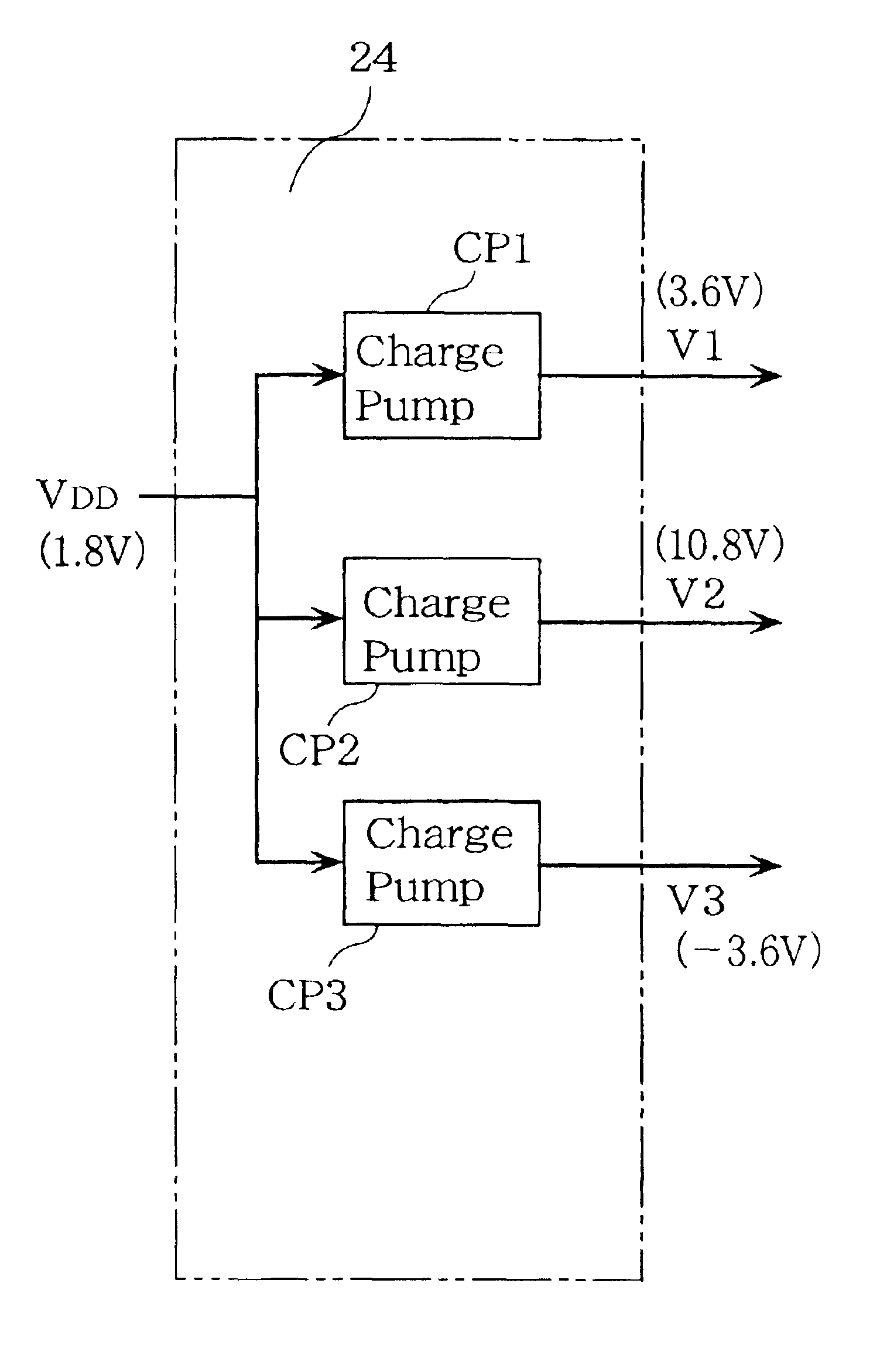
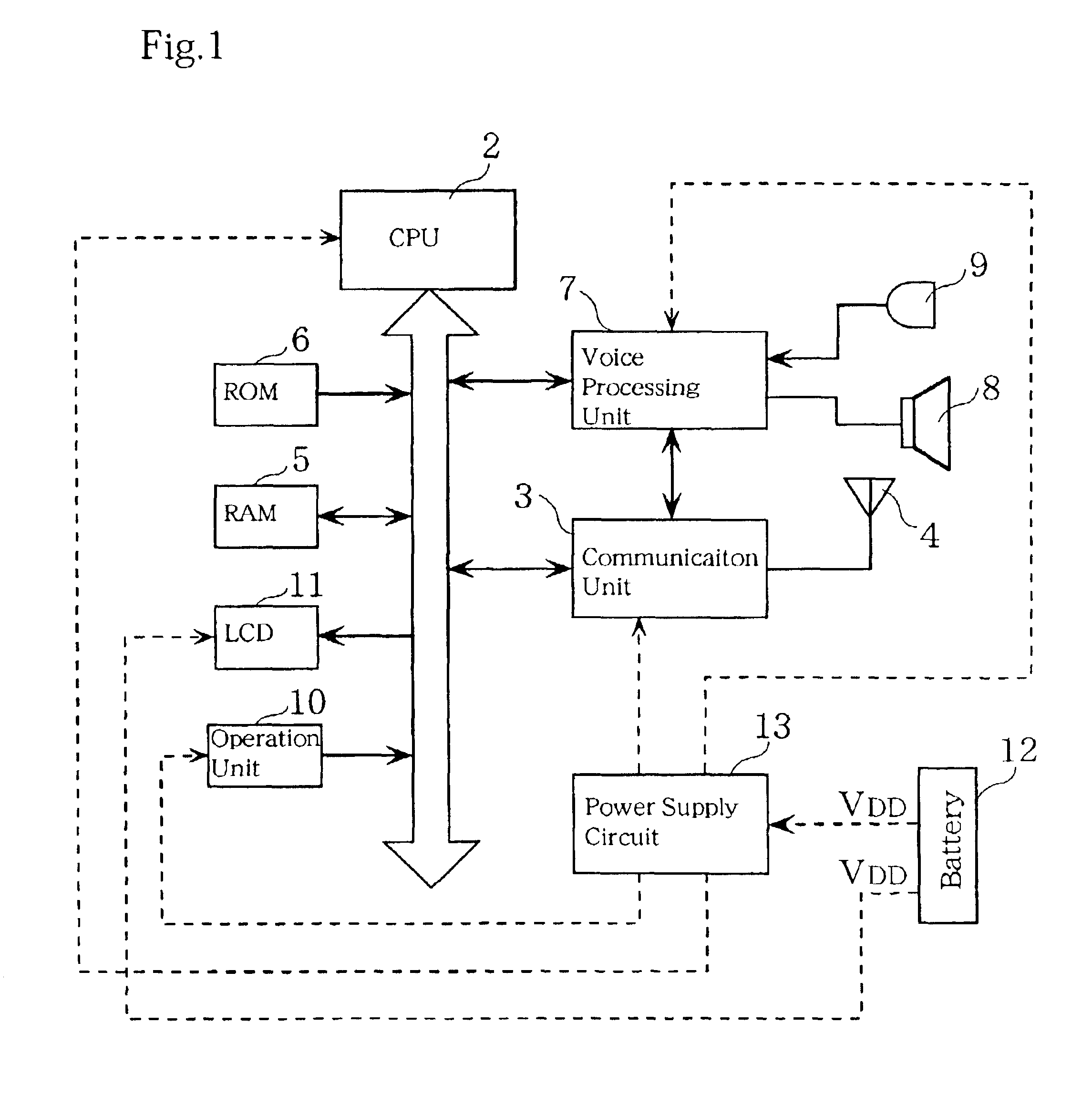
[0070]FIG. 1 is a block diagram showing the electrical configuration of a mobile phone 1 having a liquid crystal display device according to the present invention. In FIG. 1, reference numeral 2 denotes a CPU (central processing unit) for controlling the operation of each part of the mobile phone by executing phone function programs. Reference numeral 3 denotes a communication unit which is connected to an antenna 4 and which has functions of modulating transmitter signals and demodulating receiver signals. Reference numeral 5 denotes a random access memory (RAM) which is, for example, a memory for storage of user setting data or the like. Reference numeral 6 is a read only memory (ROM) in which phone function programs for reception and transmission that are executed by the CPU 2 are stored in advance. Reference numeral 7 is a voice processing unit for decoding receiver signals demodulated at the communication unit 3 and delivering voice output via a speaker 8, while at the same tim...

embodiment 2

[0101]FIG. 9 is a circuit diagram of a liquid crystal display device according to the present embodiment 2. FIG. 10 is a circuit diagram showing the configuration of a unit pixel. The liquid crystal display device of embodiment 2 is similar to that of embodiment 1 described above, and thus like numerals are accorded to corresponding parts. Embodiment 2 is characterized by the use of a system of spatial dithering. Note that digital image signals used in embodiment 2 are 4-bit data signals, which is indicative of an active matrix-type liquid crystal display device that can display 16 gray scales.

[0102]The liquid crystal display device according to the present embodiment 2 employs a system of spatial dithering and thus each of unit pixels 45 is made up of a plurality (in the present embodiment 1, four) of sub-pixels P1, P2, P3, and P4. The sub-pixel P1 has a sub-pixel electrode M1, a sub-pixel transistor Tr1 that is a thin film transistor (TFT), and a voltage controlling capacitor C1 f...

embodiment 3

[0121]The present embodiment 3 is characterized in that storage capacitors are formed in addition to the voltage controlling capacitors in each of the sub-pixels. According to such a configuration, load capacitance can be increased, and holding characteristics for the pixel electrode potentials improved. In addition, it is possible to realize an improvement in image quality.

[0122]In the following, with reference to FIGS. 15 and 16, the present embodiment is described in detail.

[0123]FIG. 15 is a diagram showing the configuration of a unit pixel in a liquid crystal display device according to embodiment 3, and FIG. 16 is an equivalent circuit diagram for a sub-pixel thereof. Parts corresponding to those of embodiment 2 are accorded like reference numerals and detailed description is omitted. In a sub-pixel P1 of a liquid crystal display device according to the present embodiment, a storage capacitor 60 is formed between the sub-pixel electrode and the upstream gate line GL, in additi...


PUM


Abstract

The present invention provides a liquid crystal display device having a liquid crystal display portion, a gate driver circuit, a source driver circuit, and a power supply circuit, where the liquid crystal display portion includes unit pixels with pixel switching elements and pixel electrodes arranged in a matrix. The pixel switching elements are thin film transistors that are made of polycrystalline silicon semiconductor formed on an insulating substrate. The power supply circuit is a charge pump-type power supply circuit, is made of a polycrystalline silicon semiconductor, and is a built-in circuit integrally formed on an insulating substrate. With such a configuration, a liquid crystal display device that greatly reduces power consumption is realized.

Description

TECHNICAL FIELD[0001]The present invention relates to a display device that is suitable for the display portion of mobile phones and the like.BACKGROUND ART[0002]Liquid crystal display devices are thin and lightweight and have low power consumption. For these reasons, use in liquid crystal displays for laptop computers and notebooks, as well as for information display portions of personal digital assistants such as mobile phones, has become widespread.[0003]Such conventional liquid crystal display devices are configured such that a required power supply voltage from an external power supply circuit is supplied to a driver circuit in the liquid crystal display panel. Specifically, a conventional power supply circuit, as shown in FIG. 21, is such that a reference voltage is stepped up to a high voltage by a booster circuit 140 including a transformer, this high voltage is divided by a voltage divider circuit 141 having a plurality of resisters (voltage divider resisters) connected in ...

Claims


Application Information

Patent Timeline
IPC IPC(8): G09G3/36G09G3/20G09G3/32H02M3/07H04M1/73
CPCG09G3/3655G09G3/3659H02M3/07G09G3/2051G09G3/2074G09G3/32G09G3/3614H04W52/027G09G2300/0876G09G2320/0219G09G2330/02G09G2330/021H02M2001/009G09G2300/0408H02M1/009Y02D30/70
Inventor NANNO, YUTAKASENDA, KOUJITAKEHASHI, SHIN-ITSU
Owner JAPAN DISPLAY CENT INC
Why Eureka
Try Eureka