Semiconductor device having a sealing resin and method of manufacturing the same

a sealing resin and semiconductor technology, applied in semiconductor devices, semiconductor/solid-state device details, electrical equipment, etc., can solve the problems of difficult connection of fine interconnects to semiconductor elements, difficult to realize large-scale inter-chip connections with high interconnect density, and poor manufacturing stability. , to achieve the effect of suppressing warpage, excellent manufacturing stability and excellent manufacturing stability

Inactive Publication Date: 2008-10-30
RENESAS ELECTRONICS CORP
View PDF25 Cites 67 Cited by
  • Summary
  • Abstract
  • Description
  • Claims
  • Application Information

AI Technical Summary

Benefits of technology

[0008]The semiconductor device of the present invention is provided with the interconnect layer, the support layer supporting the interconnect layer, and the through electrode, which extends through the support layer, connects with the interconnect layer; therefore, in the semiconductor device, it is possible to arrange the through electrode with high density. Further, since the semiconductor device has a support layer, it is possible to enhance connecting reliability between the semiconductor element and the through electrode when providing the through electrode with high density. Consequently, it is possible to realize connection of a plurality of chips or large scale inter-chip connection.
[0037]According to the present invention, a technique for connecting among a plurality of semiconductor elements with high density can be realized. Further, according to the present invention, a technique enhancing the connecting reliability among the plurality of the semiconductor elements can be realized.

Problems solved by technology

However, it has now been discovered that, in the conventional technique described in the Japanese Laid-Open Patent Publication No. 2001-345418, there is fear that bonding accuracy or quality deteriorates caused by difference of a thermal expansion coefficient between the substrate and base material of the semiconductor element.
For this reason, the connection of a fine interconnect to the semiconductor element is difficult.
Therefore, it is difficult to realize a large-scale inter-chip connection with high interconnect density.

Method used


Image

  • Semiconductor device having a sealing resin and method of manufacturing the same
  • Semiconductor device having a sealing resin and method of manufacturing the same
  • Semiconductor device having a sealing resin and method of manufacturing the same

Examples


first embodiment

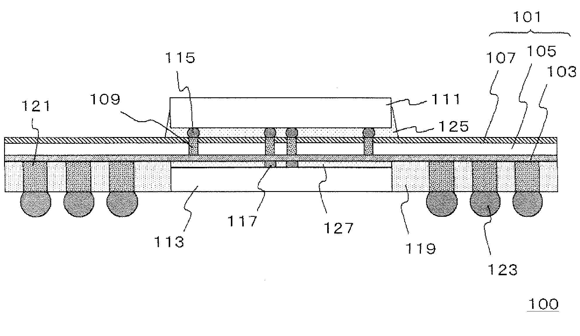
[0082]FIG. 1 is a cross-sectional view schematically showing a structure of the semiconductor device 100 according to the present embodiment. The semiconductor device 100 shown in FIG. 1 has the interconnect component 101 in the shape of a flat plate, the first semiconductor element 113 provided on a face on one side of the interconnect component 101, the insulating resin 119, which coats the face on one side where the first semiconductor element 113 of the interconnect component 101 is provided and a side face of the first semiconductor element 113, and the second semiconductor element 111 provided in such a way as to cause the second semiconductor element 111 to face to the first semiconductor element 113 on a face on the other side of the interconnect component 101.

[0083]The interconnect component 101 has a configuration where the interconnect layer 103, a silicon layer 105 and an insulating film 107 are sequentially formed into a multi-layered structure. The first semiconductor ...

second embodiment

[0125]The semiconductor device 100 (FIG. 1) described in the first embodiment is provided with the interconnect component 101 of the structure in which the interconnect layer 103, the silicon layer 105 and the insulating film 107 are sequentially formed into a multi-layered structure. However, the interconnect component 101 may be a structure composed of a multi-layered component of the interconnect layer 103 and the silicon layer 105. FIG. 7 is a cross-sectional view schematically showing a structure of a semiconductor device 110 according to the present embodiment.

[0126]A basic structure of the semiconductor device 110 shown in FIG. 7 is approximately the same as the semiconductor device 100 (FIG. 1) described in the first embodiment. The semiconductor device 110 is different from the semiconductor device 100 in that the insulating film 107 is not provided therewith, and the second semiconductor element 111 is connected with a face of the silicon layer 105 of the interconnect comp...

third embodiment

[0131]In the semiconductor device described in the above embodiments, the interconnect component 101 may be constituted of only the interconnect layer 103. FIG. 8 is a cross-sectional view schematically showing a structure of a semiconductor device 120 according to the present embodiment.

[0132]A basic structure of the semiconductor device 120 shown in FIG. 8 is approximately the same as the semiconductor device 100 (FIG. 1) described in the first embodiment. However, the semiconductor device 120 is different from the semiconductor device 100 in that the interconnect component 101 is composed of only the interconnect layer 103, and the first semiconductor element 113 and the second semiconductor element 111 are provided in such a way as to face to different faces of the interconnect layer 103. Further, the semiconductor device 120 is different from the semiconductor device 100 in that the second semiconductor element 111 is connected with a face of the interconnect layer 103 through ...


PUM


Abstract

The semiconductor device 100 comprises a first semiconductor element 113 provided on a face on one side of a flat plate shaped interconnect component 101, an insulating resin 119 covering a face of a side where the first semiconductor element 113 of the interconnect component 101 is provided and a side face of the first semiconductor element 113, and a second semiconductor element 111 provided on a face on the other side of the interconnect component 101. The interconnect component 101 has a constitution where an interconnect layer 103, a silicon layer 105 and an insulating film 107 are sequentially formed. The interconnect layer 103 has a constitution where the interconnect layer 103 has a flat plate shaped insulating component and a conductive component extending through the insulating component. The first semiconductor element 113 is electrically connected with the second semiconductor element 111 through the conductive component.

Description

[0001]This application is based on Japanese patent application NO. 2004-194690, the content of which is incorporated hereinto by reference.BACKGROUND OF THE INVENTION[0002]1. Field of the Invention[0003]The present invention relates to a semiconductor device and a method for manufacturing the same.[0004]2. Related Art[0005]As for a conventional semiconductor device, the Japanese Laid-Open Patent Publication No. 2001-345418 discloses the conventional semiconductor device. The Japanese Laid-Open Patent Publication No. 2001-345418 discloses a both-side mounting structure component in which the semiconductor device is provided on both faces of a circuit board using a flip chip mounting. According to the Japanese Laid-Open Patent Publication No. 2001-345418, improvement of a manufacturing yield and reliability may be made possible upon adjusting a glass transition temperature of a sealing resin sealing the semiconductor device after mounting.SUMMARY OF THE INVENTION[0006]However, it has ...

Claims


Application Information

Patent Timeline
Patent Type & Authority Applications(United States)
IPC IPC(8): H01L23/538H01L21/56H01L21/3205H01L21/768H01L23/522H01L25/065H01L25/07H01L25/18H01L27/00
CPCH01L21/563H01L23/3128H01L23/3135H01L23/3157H01L23/481H01L23/49816H01L23/5389H01L25/03H01L25/0657H01L25/105H01L2221/68345H01L2224/48091H01L2224/48227H01L2224/73203H01L2224/73204H01L2225/0651H01L2225/06513H01L2225/06517H01L2225/0652H01L2225/06524H01L2225/06541H01L2225/06555H01L2225/06586H01L2225/06593H01L2924/01078H01L2924/01079H01L2924/09701H01L2924/15311H01L2924/15331H01L2924/18161H01L2924/19107H01L24/48H01L2224/16145H01L2224/16225H01L2224/32225H01L2224/32145H01L2224/73265H01L2924/3511H01L25/50H01L2225/1023H01L2225/1058H01L2225/1005H01L23/5226H01L24/17H01L25/18H01L2924/1431H01L2924/1434H01L2224/16235H01L2924/00014H01L2924/00012H01L2924/00011H01L2924/00H01L2924/181H01L2924/12042H01L24/73H01L2924/14H01L2224/0401H01L2224/45099H01L2224/45015H01L2924/207H01L23/5384H01L23/5386H01L2225/06572
Inventor KURITA, YOICHIRO
Owner RENESAS ELECTRONICS CORP
Why Eureka
Try Eureka