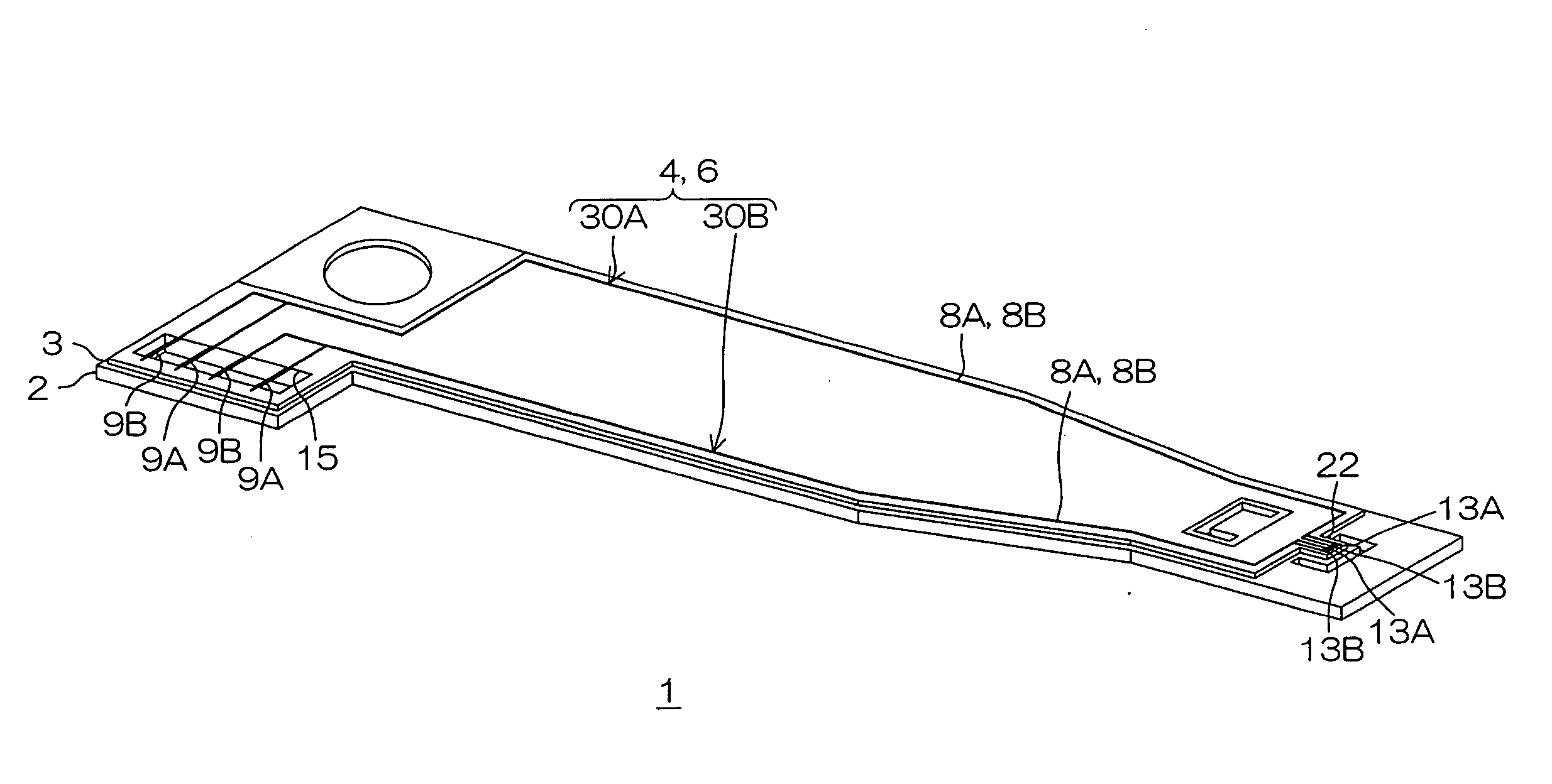
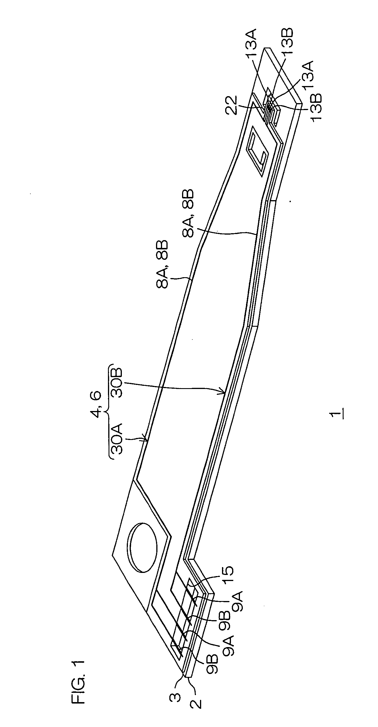
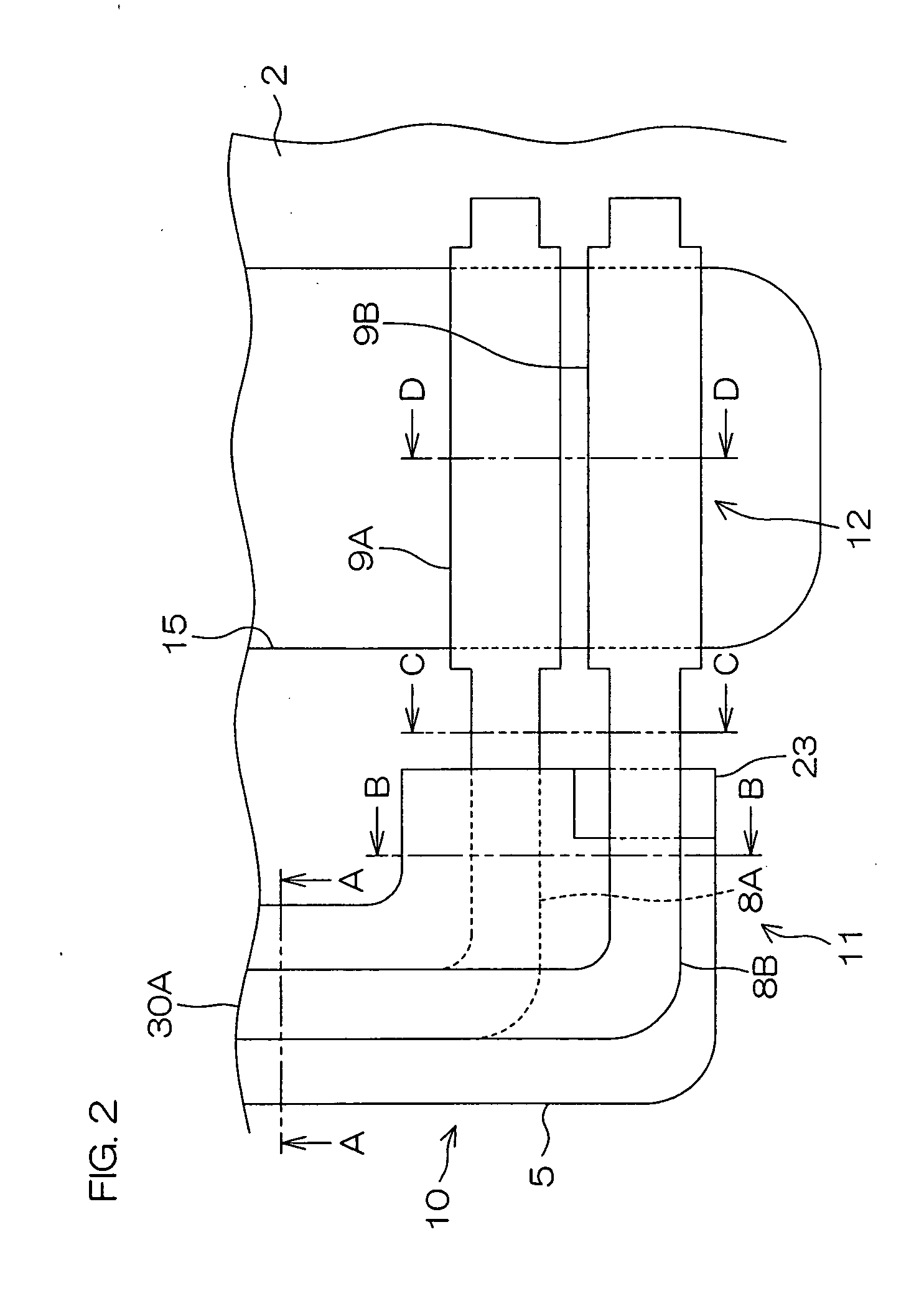
Wired circuit board

a wired circuit board and circuit board technology, applied in the field of wired circuit boards, can solve the problems of unstable impedance of the second conductor, likely wire breakage at the interface, etc., and achieve the effects of stabilizing impedance, easy connection, and stabilizing impedan

Inactive Publication Date: 2009-06-18
NITTO DENKO CORP
View PDF5 Cites 67 Cited by
  • Summary
  • Abstract
  • Description
  • Claims
  • Application Information

AI Technical Summary

Benefits of technology

[0012]It is therefore an object of the present invention to provide a wired circuit board which allows easy connection to an external terminal as well as the stabilization of impedance, and also has excellent connection reliability as well as improved flexibility in designing a first conductive layer and a second conductive layer.
[0016]In the wiring formation portion of the wired circuit board of the present invention, the second conductive layer overlaps the first conductive layer in the thickness direction. As a result, it is possible to stabilize impedance.
[0017]Additionally, in the terminal formation portion, the first conductive layer and the second conductive layer are formed in the same plane. This allows easy connection to an external terminal.
[0018]Further, in the middle portion, the second conductive layer is formed on the portion of the second insulating layer extending from the wiring formation portion to the mid-point between the wiring formation portion and the terminal formation portion, and formed continuously on the portion of the first insulating layer extending from the mid-point to the terminal formation portion. As a result, it is possible to stabilize impedance in the wiring formation portion, and achieve easy connection to the external terminal in the terminal formation portion. This allows both the stabilization of impedance and the easy connection to the external terminal.
[0019]Moreover, a terminal for connecting the first conductive layer is not needed in the middle portion, and a first external terminal portion and a second external terminal portion are formed in the same plane in the terminal formation portion. Accordingly, it is possible to prevent a wire breakage in the middle portion, and ensure excellent thermal shock resistance. As a result, excellent connection reliability can be obtained.
[0020]Furthermore, since it is not necessary to provide a terminal for connection, flexibility in designing the first conductive layer and the second conductive layer can be improved.

Problems solved by technology

However, since the second conductors mentioned above are connected to the terminals for connection via the through-hole plating portions, the problem occurs in such a way that the impedance of the second conductors becomes unstable.
This leads to the problem that a wire breakage is likely to occur at the interface.

Method used


Image

  • Wired circuit board
  • Wired circuit board
  • Wired circuit board

Examples


example 1

[0128]First, a metal supporting layer made of a stainless steel (SUS 304) foil having a thickness of 25 μm was prepared (see FIG. 6(a)). Then, a varnish of a photosensitive polyamic acid resin was coated on the entire upper surface of the metal supporting layer, dried, and exposed to light via a gradation exposure photomask to form a first base coating. Subsequently, the first base coating was developed, and further cured by heating to form a first insulating base layer made of polyimide having a thickness of 3 μm (see FIG. 6(b)). In the first insulating base layer, a base depressed portion having a thickness of 1 μm was formed.

[0129]Then, a first conductive layer was formed on the insulating base layer by an additive method.

[0130]In the additive method, a chromium thin film having a thickness of 0.03 μm, and a copper thin film having a thickness of 0.07 μm were successively formed as a first metal thin film by chromium sputtering and copper sputtering on the entire upper surface of...


PUM


Abstract

A wired circuit board includes a wiring formation portion, a terminal formation portion, and a middle portion formed therebetween. The wiring formation portion includes a first conductive layer formed on a first insulating layer, and a second conductive layer formed on a second insulating layer so as to overlap the first conductive layer in a thickness direction. The terminal formation portion includes the first and second conductive layers formed in parallel in the same plane. The middle portion includes the first conductive layer formed on the first insulating layer, and the second conductive layer formed on a portion of the second insulating layer extending from the wiring formation portion to a mid-point between the wiring formation portion and the terminal formation portion, and formed on a portion of the first insulating layer extending from the mid-point to the terminal formation portion.

Description

CROSS-REFERENCE TO RELATED APPLICATIONS[0001]This application claims the benefit of U.S. Provisional Application No. 60 / 996,753, filed Dec. 4, 2007, and claims priority from Japanese Patent Application No. 2007-302026, filed Nov. 21, 2007, the contents of which are herein incorporated by reference in their entirety.BACKGROUND OF THE INVENTION[0002]1. Field of the Invention[0003]The present invention relates to a wired circuit board and, more particularly, to a wired circuit board such as a suspension board with circuit or a flexible wired circuit board.[0004]2. Description of the Related Art[0005]In recent years, to respond to an increase in wiring density, it has been known to use a double-decker structure in which one wire and the other wire are disposed to oppose each other with an insulating layer interposed therebetween in a thickness direction as a wiring structure in a wired circuit board such as a suspension board with circuit or a flexible wired circuit board.[0006]For exam...

Claims


Application Information

Patent Timeline
Patent Type & Authority Applications(United States)
IPC IPC(8): H05K1/11
CPCG11B5/486H05K1/0245H05K1/025H05K2201/0969H05K1/112H05K2201/0394H05K2201/09672H05K1/056G11B5/484
Inventor OHSAWA, TETSUYAKAMEI, KATSUTOSHI
Owner NITTO DENKO CORP
Why Eureka
Try Eureka