Single-chip imager system with programmable dynamic range

a single-chip imager and dynamic range technology, applied in the field of image sensors, can solve the problems of reducing the dynamic range of cmos imagers, the limiting performance characteristic of imagers, and the inability to provide sufficient degree of dynamic range expansion, etc., to achieve elegantly simple input/output connections and cost-effective production

Inactive Publication Date: 2005-12-20
MASSACHUSETTS INST OF TECH
View PDF31 Cites 245 Cited by
  • Summary
  • Abstract
  • Description
  • Claims
  • Application Information

AI Technical Summary

Benefits of technology

[0028]The integration control method and the imager system provided by the invention can be adapted for a wide range of imager applications and configurations, including machine vision and scientific applications such as automotive and astronomy applications, as well as consumer applications such as camcorder and still camera products. The imager system can be produced cost-effectively and with elegantly simple input / output connections. User-programmability enables real time flexibility that accommodates the demands of many applications.

Problems solved by technology

The reduced dynamic range of CMOS imagers is generally due to a readout noise level that is higher than that of CCD imagers.
This performance limitation of CMOS imagers results in a required trade-off between operational and functional features together desired of an image sensor for a given application.
For applications such as vehicle-based imaging systems that inherently have no control over natural or artificial light in a scene to be imaged, the dynamic range of an imager can be the limiting performance characteristic of the imager.
In general such techniques are found to provide an inadequate degree of dynamic range expansion, to require a tradeoff with spatial resolution, frame rate, size, cost or other image sensor consideration, or to impose excessive operational requirements.
As a result, the multifaceted demands of many imager applications have generally not been fully addressed in a single imager system.

Method used


Image

  • Single-chip imager system with programmable dynamic range
  • Single-chip imager system with programmable dynamic range
  • Single-chip imager system with programmable dynamic range

Examples


Embodiment Construction

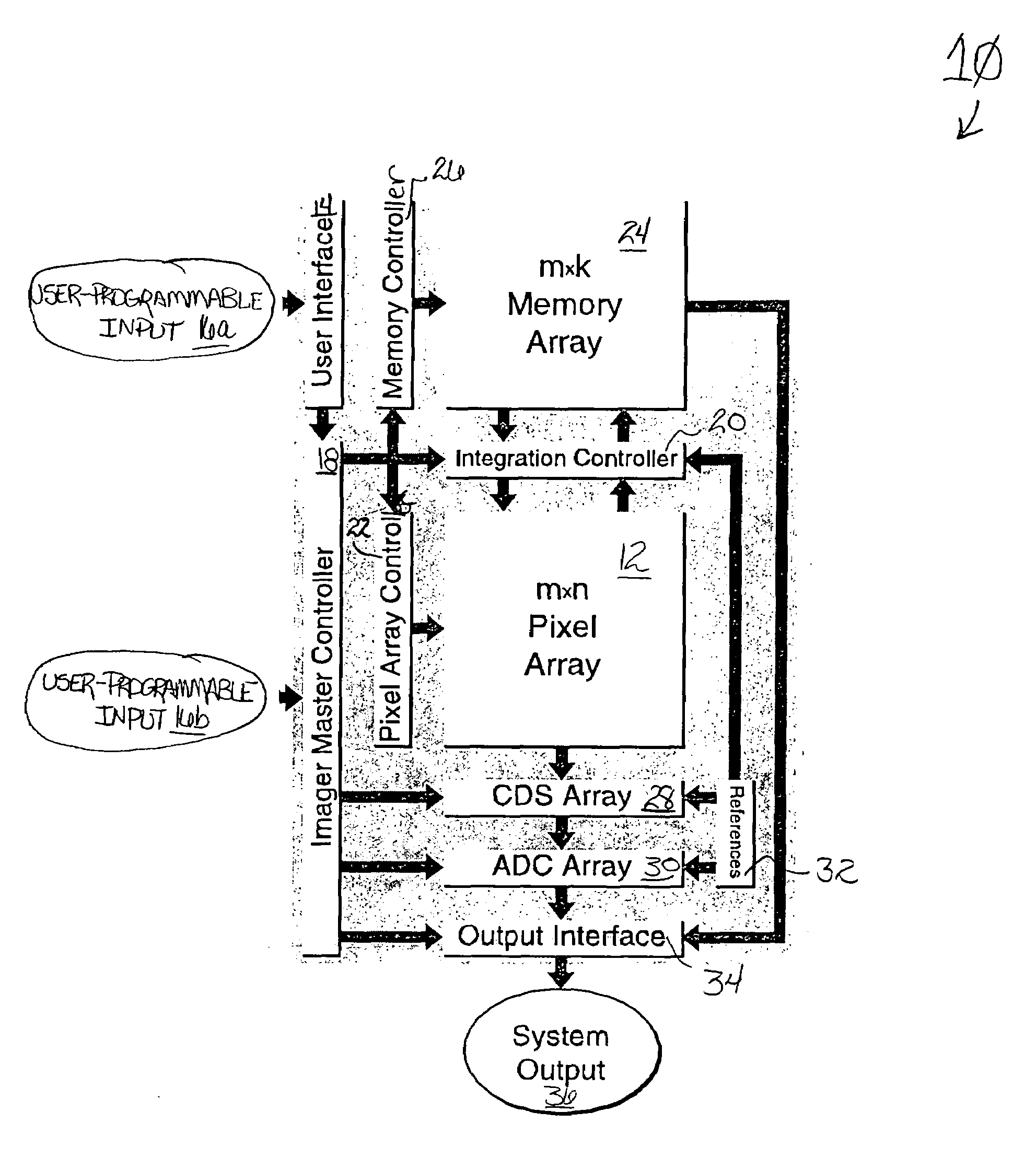
[0060]Referring to FIG. 1, there is shown an example imager system 10 provided by the invention. The imager system includes a pixel array 12 having a number, m, of pixel rows and a number, n, of pixel columns. This array can consist of, e.g., CMOS pixels, CCD pixels, or other selected pixel technology. The specific example provided here will be directed to CMOS pixel technology, but it is to be recognized that the imager system of the invention is not limited to such. Whatever pixel technology is employed, the pixel array is configured to enable exposure of the array to a scene for capture of illumination for producing an image of the scene.

[0061]In accordance with the invention, all of the pixels in the array can be independently reset and further can be non-destructively read. These features enable the pixel-specific and user-programmable dynamic range control of the invention described below. The user interface 14 of the system provides an abstraction layer between a user and the...


PUM


Abstract

The imager system of the invention, provided in a semiconductor substrate, includes a plurality of photosensitive, charge integrating pixels that are arranged in rows and columns of a pixel array for capturing illumination of a scene to be imaged. Each pixel includes a photogenerated charge accumulation region of the semiconductor substrate and a sense node at which an electrical signal, indicative of pixel charge accumulation, can be measured without discharging the accumulation region. Pixel access control circuitry is connected to pixel array rows and columns to deliver pixel access signals generated by the access control circuitry for independently accessing a selected pixel in the array. An input interface circuit is connected to accept a dynamic range specification input for the array pixels. Integration control circuitry is connected to access a selected pixel of the array to read the sense node electrical signal of the selected pixel, and configured to generate pixel-specific integration control signals delivered to the selected pixel, independent of other pixels, based on dynamic range specification input provided by the input interface circuit. An output interface circuit is connected to the pixel array to produce output image data based on sense node electrical signals from the pixel array.

Description

[0001]This application claims the benefit of U.S. Provisional Application No. 60 / 121,845, filed Feb. 26, 1999, the entirety of which is incorporated by reference.[0002]This invention was made with funds from the U.S. government under contract No. MIP-9423221 administered by the National Science Foundation. The government has certain rights in the invention.BACKGROUND OF THE INVENTION[0003]This invention relates to image sensors and more particularly relates to methods for controlling the dynamic range of an image sensor.[0004]CMOS image sensors are increasingly becoming the preferable selection over CCD image sensors for a wide range of solid-state imaging applications. This is particularly true for those applications that demand the inherent advantages of CMOS fabrication such as low cost, small feature size production, and large-scale monolithic integration. But because the illumination range, or dynamic range, characteristic of CCD image sensors is generally larger than that of C...

Claims


Application Information

Patent Timeline
Patent Type & Authority Patents(United States)
IPC IPC(8): H04N3/14H04N5/353H04N5/355H04N5/374H04N5/378
CPCH04N5/2355H04N5/335H04N23/741H04N25/00
Inventor ACOSTA-SERAFINI, PABLO M.MASAKI, ICHIROSODINI, CHARLES G.
Owner MASSACHUSETTS INST OF TECH
Why Eureka
Try Eureka