High-frequency switching transistor and high-frequency circuit

a high-frequency switching and high-frequency circuit technology, applied in the field of high-frequency mos transistors, can solve the problems of difficult integration with a unitary semiconductor technology, such as a pure silicon technology, and the limited switchable power of the available bias voltage, so as to reduce the (inner) resistance, reduce the resistance, and reduce the breakdown strength

Active Publication Date: 2006-06-08
INFINEON TECH AG
View PDF11 Cites 43 Cited by
  • Summary
  • Abstract
  • Description
  • Claims
  • Application Information

AI Technical Summary

Benefits of technology

[0015] It is an object of the present invention to provide a high-frequency switch, which has better integration characteristics compared to conventional high-frequency switches and can be produced in a more cost-effective way.

Problems solved by technology

Thereby, the switchable power of the available bias voltage is limited.
However, the higher costs are disadvantageous, which are incurred by the additional parts and which make an integration with a unitary semiconductor technology, such as a pure silicon technology, more difficult.
Both technologies are more expensive than Si technology.

Method used


Image

  • High-frequency switching transistor and high-frequency circuit
  • High-frequency switching transistor and high-frequency circuit
  • High-frequency switching transistor and high-frequency circuit

Examples


Embodiment Construction

[0050] In the figures, equal or similar reference numbers are used for equal or similar elements, wherein a repeated description of these reference numbers is omitted.

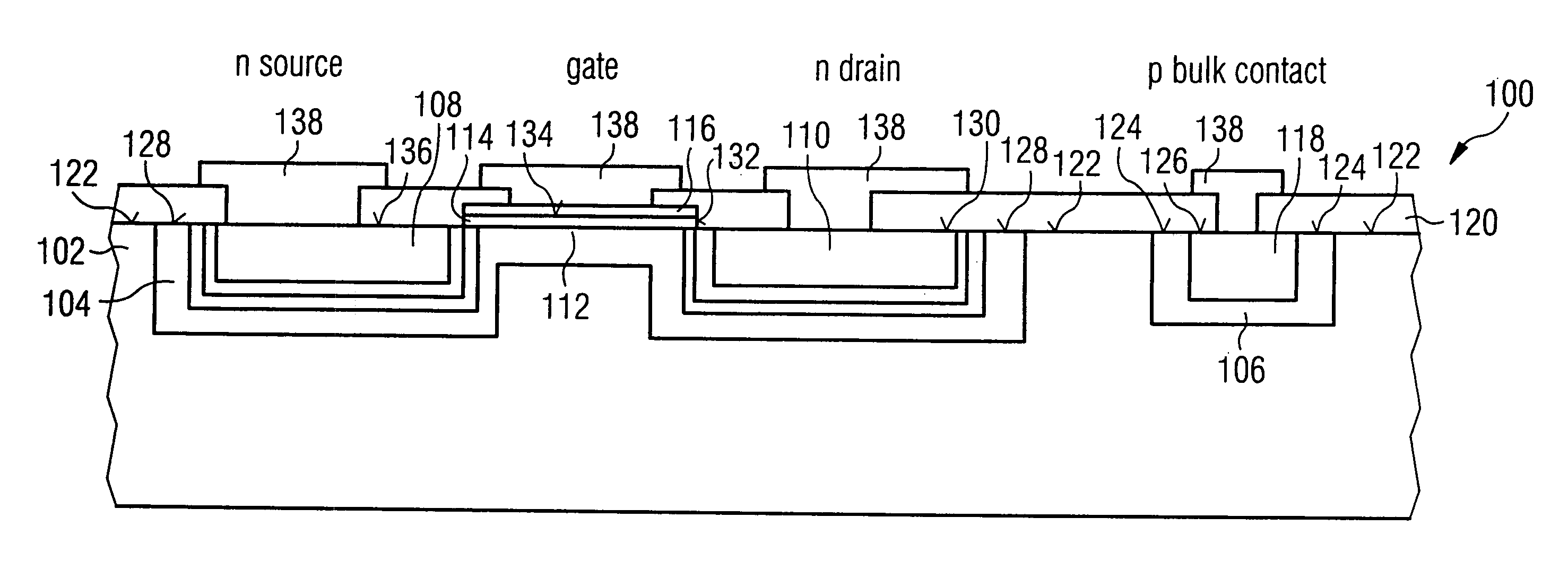
[0051]FIG. 1a shows a high-frequency switching transistor 100, having a substrate 102 as well as barrier region 104 embedded in the substrate 102 and a further barrier region 106 embedded in the substrate 102. The substrate 102 can be a semi-insulating semiconductor material, wherein conventional semiconductor substrates with p doping and a substrate doping concentration of, for example, less than 1014 dopant atoms per cubic centimeter can be used for such a substrate 102. For the barrier region 104, for example, dopant atoms for a p doping can be introduced into the substrate 102, so that the dopant concentration of the barrier region (i.e. the barrier region dopant concentration) is higher than the substrate dopant concentration. Thereby, the barrier region dopant concentration can be preferably in a range of values...


PUM


Abstract

A high-frequency switching transistor comprises a substrate having a substrate dopant concentration and a barrier region bordering on the substrate, which has a first conductivity type, wherein a barrier region dopant concentration is higher than the substrate dopant concentration. Further, the high-frequency switching transistor comprises a source region embedded in the barrier region, which comprises a second conductivity type different to the first conductivity type, and has a source region dopant concentration, which is higher than the barrier region dopant concentration. Additionally, the high-frequency switching transistor comprises a drain region embedded in the barrier region and disposed offset from the source region, which comprises the second conductivity type and has a drain region dopant concentration, which is higher than the barrier region dopant concentration. Further, the high-frequency switching transistor has a channel region, extending between the source region, wherein the channel region comprises a subregion of the barrier region. Further, the high-frequency switching transistor has an insulation region, which covers the channel region and which is disposed between the channel region and the gate electrode. Such a high-frequency switching transistor allows switching of high-frequency signals with higher high-frequency signal amplitudes as are switchable by conventional high-frequency switching transistors.

Description

CROSS-REFERENCE TO RELATED APPLICATION [0001] This application claims priority from German Patent Application No. 102004053558.2, which was filed on Nov. 5, 2004, German Patent Application No. 102004061561.6, which was filed on Dec. 21, 2004, and German Patent Application No. 102005049247.9, which was filed on Oct. 14, 2005, all of which are incorporated herein by reference in its entirety. BACKGROUND OF THE INVENTION [0002] 1. Field of the Invention [0003] The present invention relates to the technical field of semiconductor electronics and particularly to the technical partial field of high-frequency MOS transistors. [0004] 2. Description of the Prior Art [0005] High-frequency switches have the task to pass or block high-frequency signals. In the passing case, the same should be characterized by an ohmic resistance, which is as small as possible, and in the blocking case, by a constant capacity, which is as small as possible. They can be realized by different types of switching el...

Claims


Application Information

Patent Timeline
Patent Type & Authority Applications(United States)
IPC IPC(8): H01L29/76
CPCH01L27/088H01L29/1083H01L29/1087H03K17/6871H03K17/693
Inventor LOSEHAND, REINHARDTADDIKEN, HANSGERLACH, UDO
Owner INFINEON TECH AG
Why Eureka
Try Eureka