In-situ hybrid deposition of high dielectric constant films using atomic layer deposition and chemical vapor deposition

Inactive Publication Date: 2009-10-01
TOKYO ELECTRON LTD
View PDF40 Cites 313 Cited by
  • Summary
  • Abstract
  • Description
  • Claims
  • Application Information

AI Technical Summary

Benefits of technology

[0005]Embodiments of the invention provide a method for in-situ hybrid deposition of a high-k dielectric film on a plurality of substrates for high-volume semiconductor manufacturing. The method includes sequential deposition of the high-k dielectric film using atomic layer deposition (ALD) and chemical vapor deposition (CVD). The portion of the high-k dielectric film deposited by ALD forms an excellent interface with the underlying substrate or an interface lay

Problems solved by technology

Among the more established techniques are Chemical Vapor Deposition (CVD) and Atomic Layer Deposition (ALD), but these dep

Method used


Image

  • In-situ hybrid deposition of high dielectric constant films using atomic layer deposition and chemical vapor deposition
  • In-situ hybrid deposition of high dielectric constant films using atomic layer deposition and chemical vapor deposition
  • In-situ hybrid deposition of high dielectric constant films using atomic layer deposition and chemical vapor deposition

Examples


Example

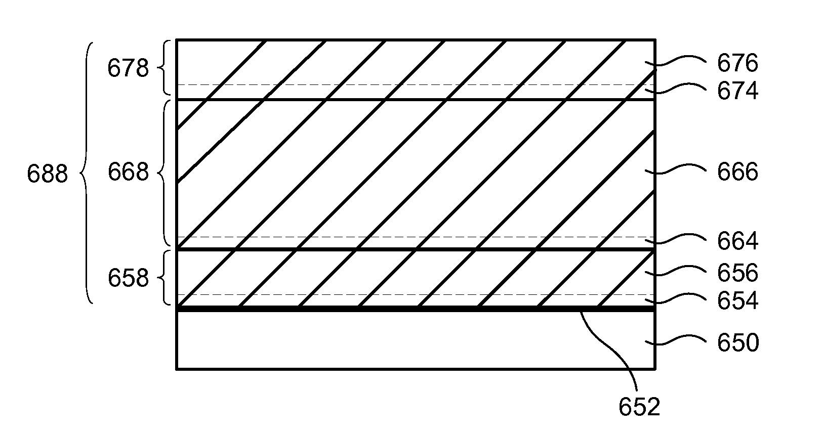
[0015]Several methods have previously been developed for creating thin high-k dielectric films on substrates used in manufacturing semiconductor devices. Among the more established techniques is CVD. ALD, a variant of CVD, is a relatively newer technology now emerging as a potentially superior method of achieving uniform, conformal film deposition. ALD is a slower deposition method than CVD due to lower film deposition rates. However, ALD often provides superior high-k dielectric film properties such as better film conformality over high-aspect-ratio features such as trenches or vias commonly found in semiconductor devices, and reduced leakage currents due at least in part to better interfaces between the high-k dielectric film and underlying substrate and / or other films. Many uses of high-k dielectric films in semiconductor devices require film thicknesses that make ALD very time consuming due to the low film deposition rate and ALD can therefore be prohibitively expensive to perfo...


PUM

PropertyMeasurementUnit
Temperatureaaaaaaaaaa

Abstract

An in-situ hybrid film deposition method for forming a high-k dielectric film on a plurality of substrates in a batch processing system. The method includes loading the plurality of substrates into a process chamber of the batch processing system, depositing by atomic layer deposition (ALD) a first portion of a high-k dielectric film on the plurality of substrates, after depositing the first portion, and without removing the plurality of substrates from the process chamber, depositing by chemical vapor deposition (CVD) a second portion of the high-k dielectric film on the first portion, and removing the plurality of substrates from the process chamber. The method can further include alternatingly repeating the deposition of the first and second portions until the high-k dielectric film has a desired thickness. The method can still further include pre-treating the substrates and post-treating the high-k dielectric film in-situ prior to the removing.

Description

CROSS-REFERENCE TO RELATED APPLICATIONS[0001]The present invention is related to U.S. patent application Ser. No. 11 / 462,234, filed Aug. 3, 2006 and entitled IN-SITU ATOMIC LAYER DEPOSITION. The entire content of this application is incorporated herein by reference.FIELD OF THE INVENTION[0002]This invention relates to deposition of high dielectric constant (high-k) dielectric films for microelectronic devices, and more particularly to an in-situ hybrid deposition of high-k dielectric films using a combination of atomic layer deposition (ALD) and chemical vapor deposition (CVD).BACKGROUND OF THE INVENTION[0003]In the semiconductor industry, the minimum feature sizes of microelectronic devices are well into the deep sub-micron regime to meet the demand for faster, and lower power semiconductor devices. The downscaling of complimentary metal-oxide-semiconductor (CMOS) devices imposes scaling constraints on the gate dielectric material. The thickness of the conventional SiO2 gate dielec...

Claims


Application Information

Patent Timeline
IPC IPC(8): H01L21/31
CPCC23C16/02H01L21/31645C23C16/44C23C16/45546C23C16/56H01L21/02181H01L21/02271H01L21/0228H01L21/02312H01L21/02337H01L21/3141H01L21/3144H01L21/3162H01L21/31637H01L21/31641C23C16/405
Inventor REID, KIMBERLY G.DIP, ANTHONY
Owner TOKYO ELECTRON LTD
Why Eureka
Try Eureka