Schottky barrier diode and method of making the same

a diode and shielding technology, applied in the field of schottky barrier power rectifier, can solve the problems of requiring a complex process of at least four to six masks, and a larger reverse recovery time than the typical schottky barrier rectifier

Active Publication Date: 2005-10-20
WU SHYE LIN +1
View PDF2 Cites 73 Cited by
  • Summary
  • Abstract
  • Description
  • Claims
  • Application Information

AI Technical Summary

Benefits of technology

[0011] In the third preferred embodiment, the processes include using a hard mask defining first trenches and termination trenches and performing an ion implant to form p-regions. The hard mask is then removed. An anneal process to form a thermal oxide lining is then followed. Thereafter, a silicon layer is deposited to fill in the first trenches and over the uppermost surface of the thermal oxide lining to a predetermined thickness. A thermal oxidation is then carried out to oxidize the silicon layer out of the first trenches. Then the active region defined, the metallization process, and the anode electrode formation, cathode electrode formation are the same as the first preferred embodiment.
[0012] In the fourth preferred embodiment, the processes are similar to the third preferred embodiment but the active region includes all of the first trenches from a cross-sectional view. Then the metallization process, and the anode electrode formation, cathode electrode formation are the same as the second preferred embodiment.
[0048] The Schottky diode according the present invention is a trench-type, which generally has higher breakdown voltage than conventional planar-type Schottky diode.

Problems solved by technology

However, it requires a complex processes at least four to six masks.
And also, the buried p-n junctions will introduce many minority carriers when device is under forward bias, which will result in a larger reverse recovery time than the typical Schottky barrier rectifier.

Method used


Image

  • Schottky barrier diode and method of making the same
  • Schottky barrier diode and method of making the same
  • Schottky barrier diode and method of making the same

Examples


Embodiment Construction

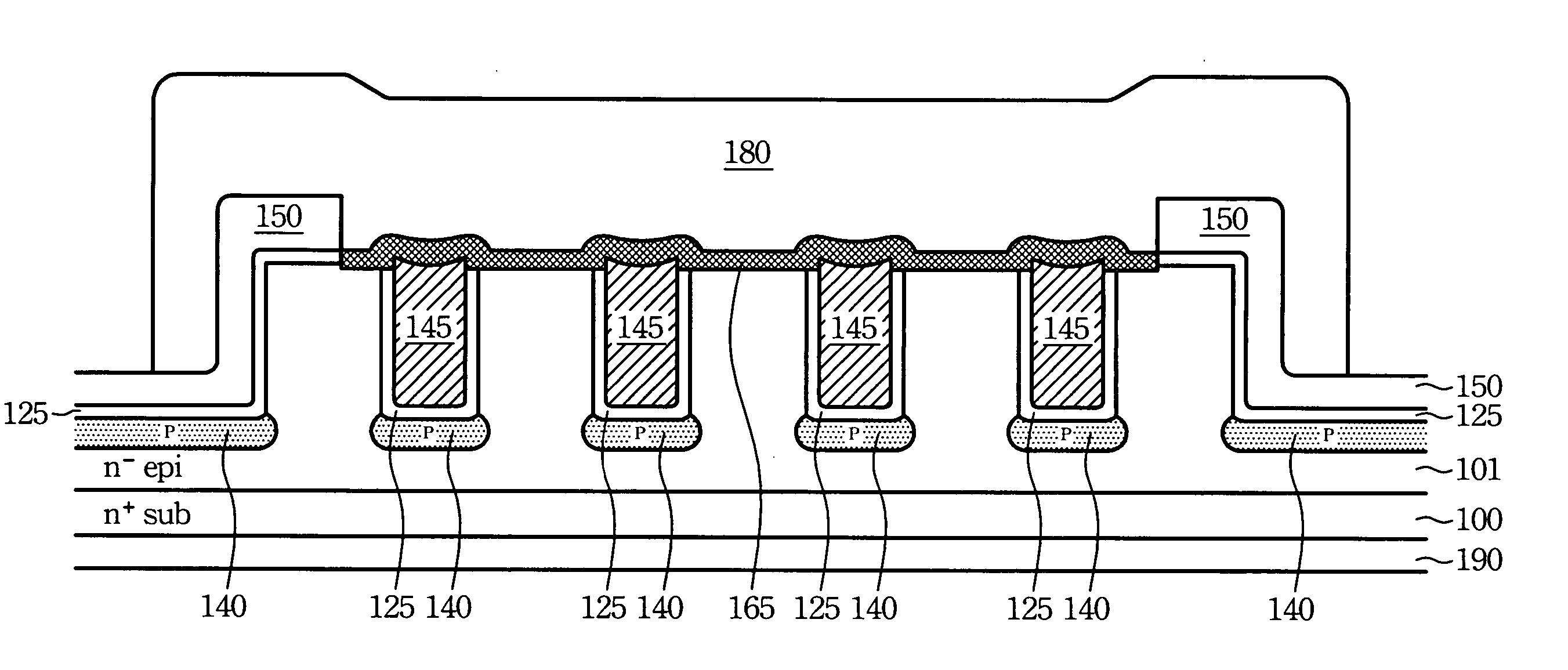
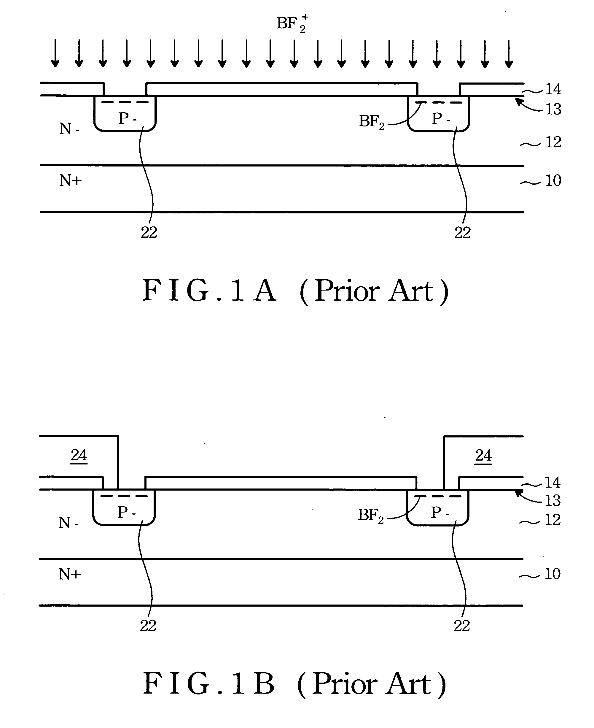
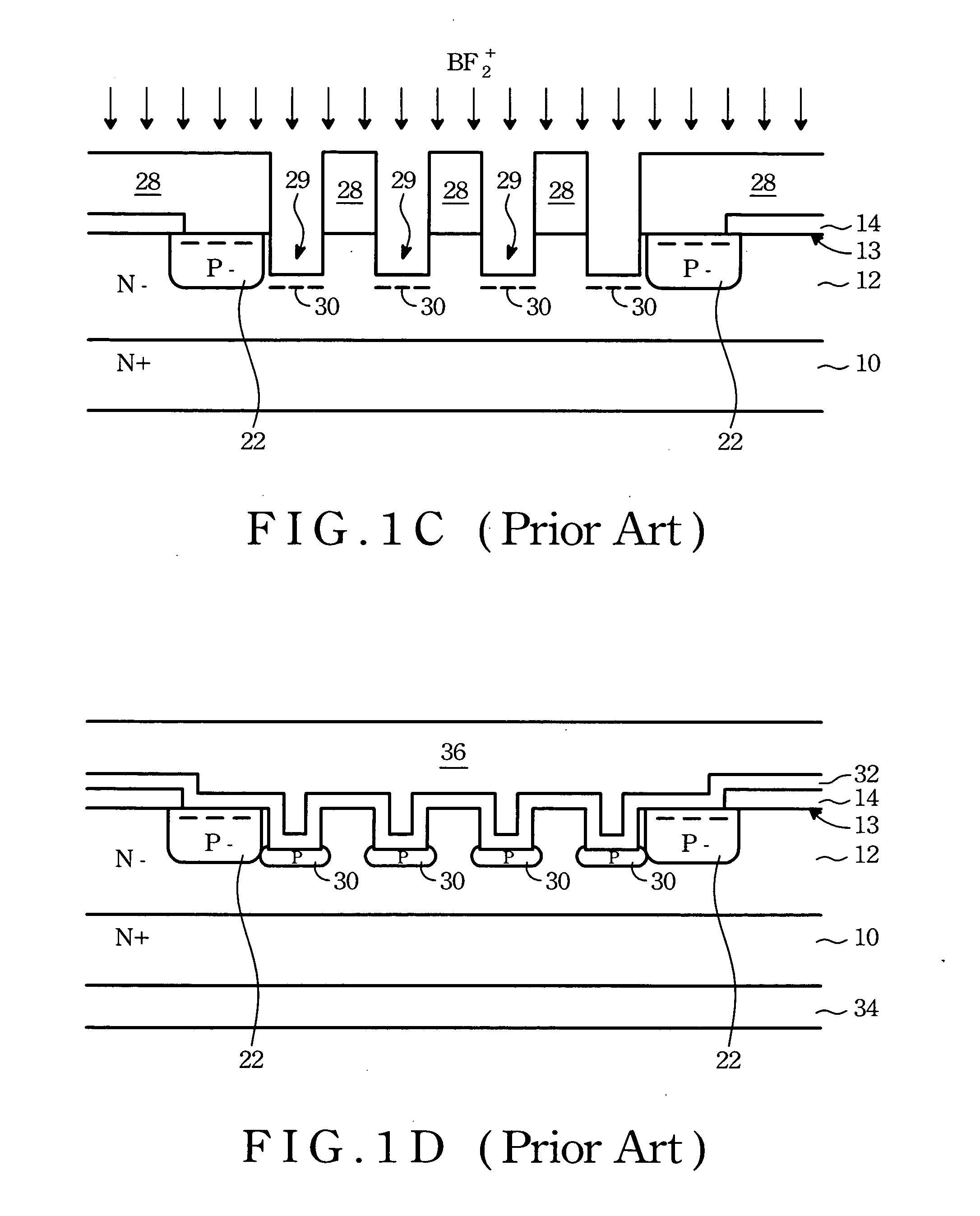
[0031] As depicted in the forgoing background of the invention, to form a power rectifier device and its termination structure using the conventional technique requires at least four to six photo masks. The present invention can simplify the processes by using only three photo masks. The detailed descriptions are as follows:

[0032] Firstly, an n+ doped substrate 100 formed with an n− drift layer 101 is provided. To define trenches, referring to FIG. 2A, an ONO stack layer formed of a pad oxide layer 110, a nitride layer 120, and a thick oxide layer 130 is formed on the n− drift layer 101. Preferably, the layers 110, 120, and 130, are, respectively, between about 5 to 100 nm, 50-300 nm, and 0 to 1000 nm in thickness. A lithographic technique and etching steps are then performed to pattern the ONO stack layer so as to define a hard mask having opening 135, and 135A.

[0033] Referring to FIG. 2B, an etching step is then performed to form first trenches 135, and termination trenches 135A...


PUM


Abstract

A power Schottky rectifier device having a plurality of first trenches filled in with an un-doped polycrystalline silicon layer and each first trenches also has a p-region beneath the bottom of said first trenches to block out reverse current while a reverse biased is applied and to reduce minority carrier while forward biased is applied. Thus, the power Schottky rectifier device can provide first fast switch speed. The power Schottky rectifier device is formed with termination region at an outer portion of the substrate. The manufacture method is also provided.

Description

FIELD OF THE INVENTION [0001] The present invention relates to a semiconductor process, specifically, to a Schottky barrier power rectifier having buried p-region beneath un-doped polycrystalline trench structure to reduce reverse leakage current, and improve breakdown voltage, and reduce minority current while forward biased, which results in a high switching speed. BACKGROUND OF THE INVENTION [0002] Schottky diode is an important power device and used extensively as output rectifiers in switching-mode power supplies and in other high-speed power switching applications, such as motor drives, switching of communication device, industry automation and electronic automation and so on. The power devices are usually required characteristics of carrying large forward current, high reverse-biased blocking voltage, such as above 100 volt, and minimizing the reverse-biased leakage current. [0003] A number of power rectifiers have been used to provide high current and reverse blocking charac...

Claims


Application Information

Patent Timeline
Patent Type & Authority Applications(United States)
IPC IPC(8): H01L21/329H01L21/336H01L29/872H01L31/062
CPCH01L29/0623H01L29/8725H01L29/872H01L29/66143
Inventor WU, SHYE-LIN
Owner WU SHYE LIN
Why Eureka
Try Eureka