Trench-Based Power Semiconductor Devices With Increased Breakdown Voltage Characteristics

a technology of breakdown voltage and semiconductor devices, which is applied in the direction of semiconductors, electrical devices, transistors, etc., can solve the problems of increasing the total die area and cost of the die, affecting the production efficiency of the die, etc., to achieve the effect of increasing the breakdown voltag

Active Publication Date: 2010-06-10
SEMICON COMPONENTS IND LLC
View PDF101 Cites 78 Cited by
  • Summary
  • Abstract
  • Description
  • Claims
  • Application Information

AI Technical Summary

Benefits of technology

[0005]The inventors have discovered several locations in trench-based power devices where parasitic breakdown conditions are likely to occur first. The present application provides novel and inventive features that counter these breakdown conditions and increase breakdown voltage.

Problems solved by technology

However, there are various breakdown processes that can occur in the field termination area and inactive area at significantly lower voltages.
However, such prior art designs often fall short of this goal, often requiring compromises that increase the total die area and cost of the die.

Method used


Image

  • Trench-Based Power Semiconductor Devices With Increased Breakdown Voltage Characteristics
  • Trench-Based Power Semiconductor Devices With Increased Breakdown Voltage Characteristics
  • Trench-Based Power Semiconductor Devices With Increased Breakdown Voltage Characteristics

Examples


Embodiment Construction

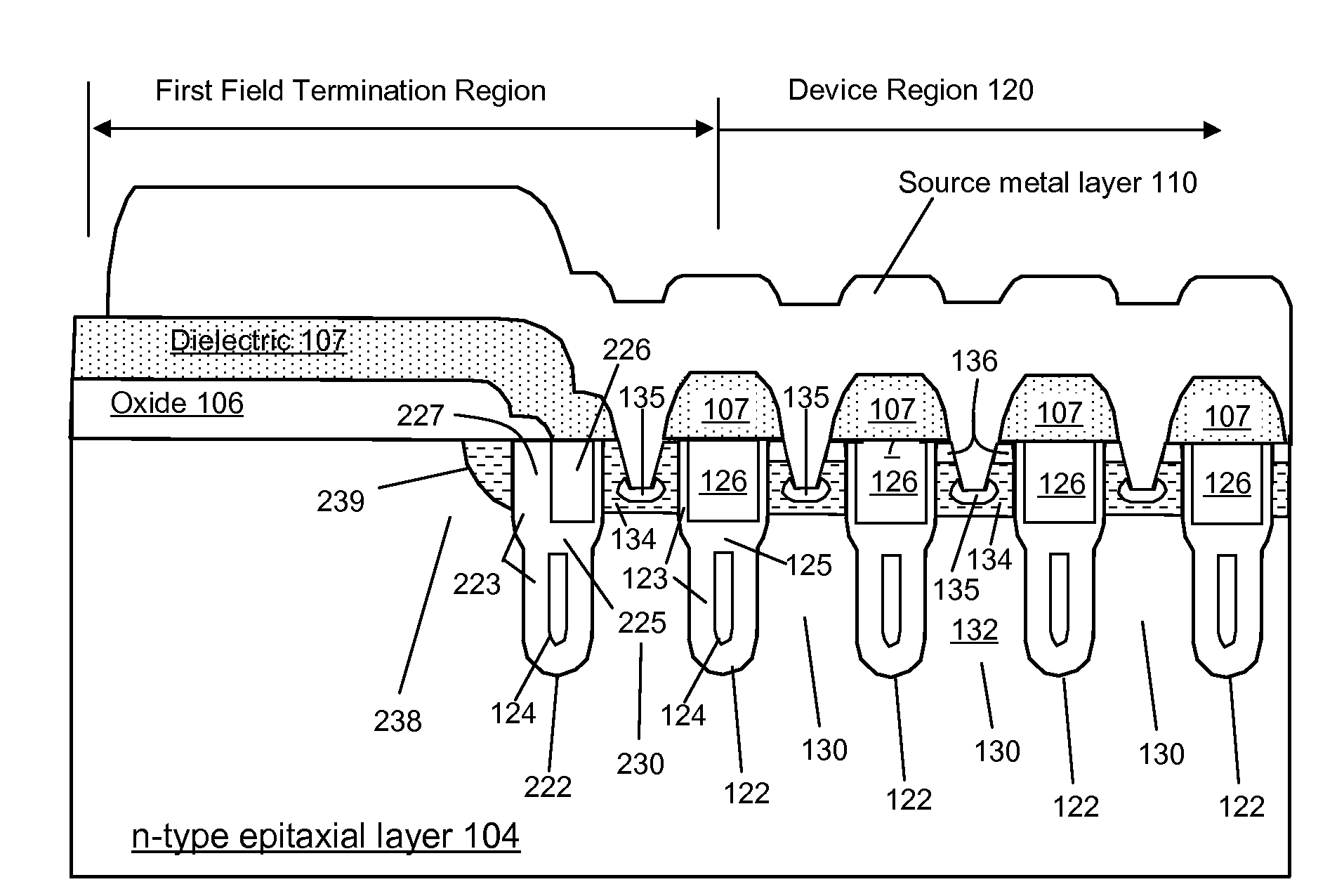
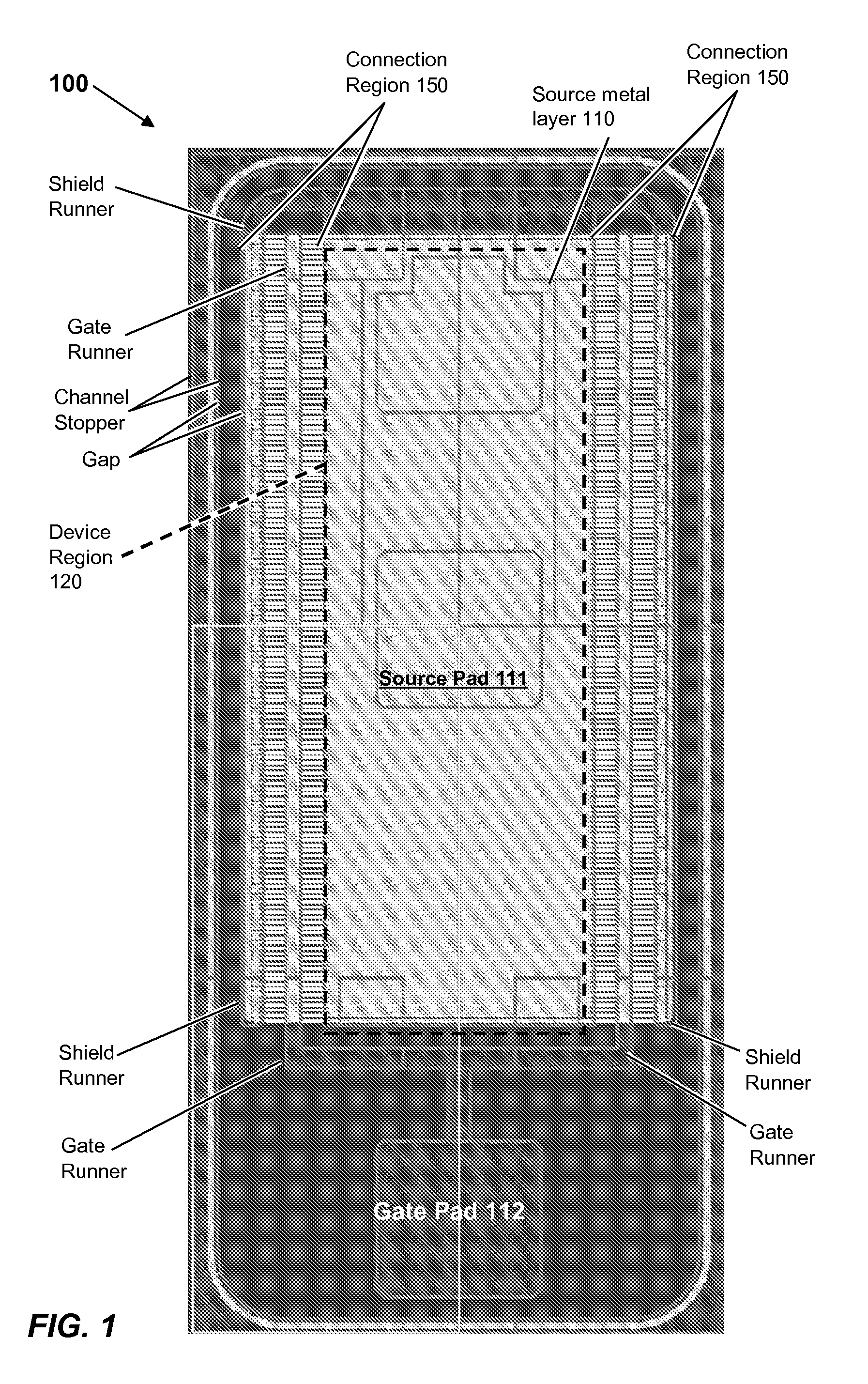
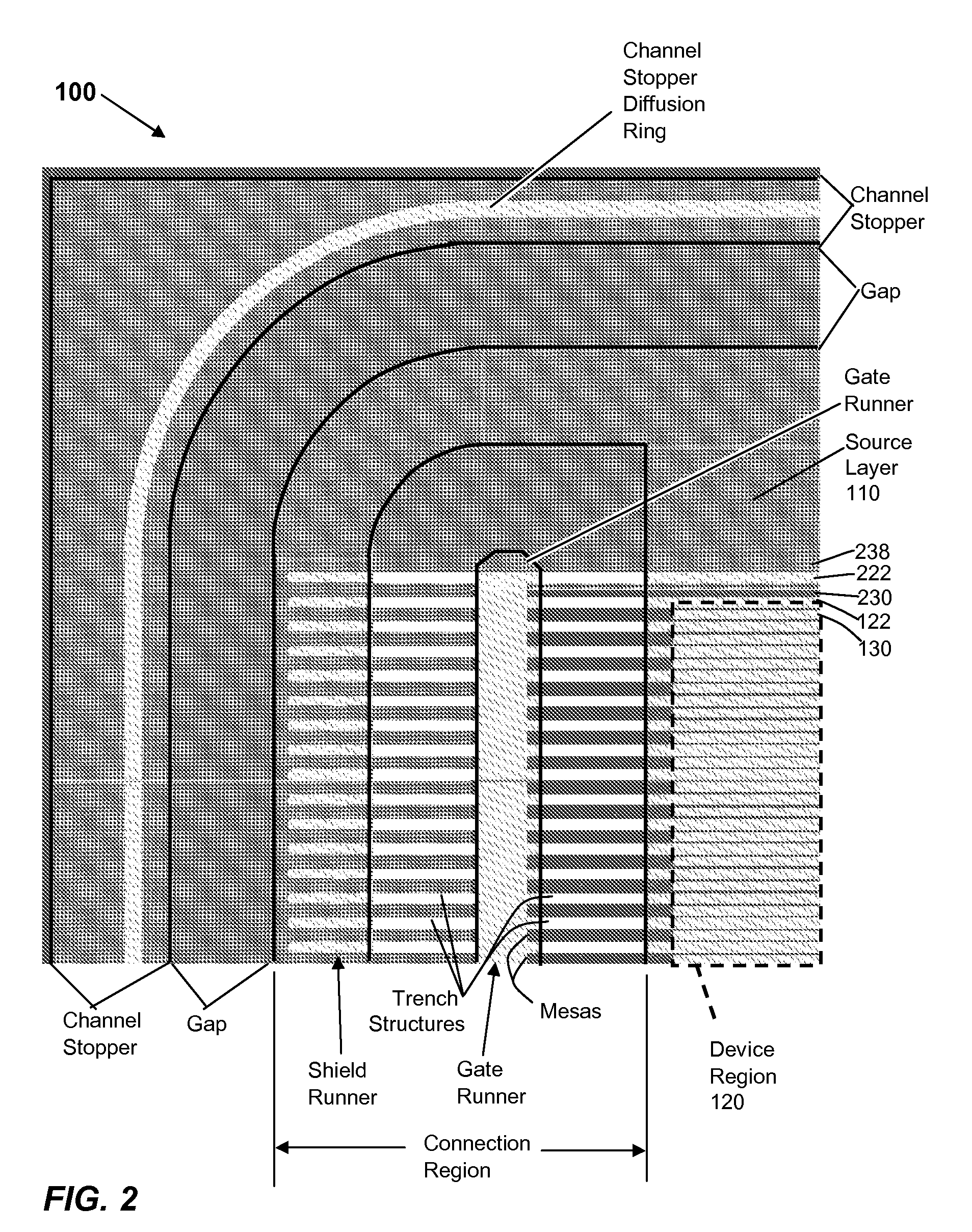
[0022]The techniques in accordance with the present inventions will be described more fully hereinafter with reference to the accompanying drawings, in which exemplary embodiments of the invention are shown. This invention may, however, be embodied in different forms and should not be construed as limited to the embodiments set forth herein. Rather, these embodiments are provided so that this disclosure is thorough and complete and fully conveys the scope of the invention to one skilled in the art. In the drawings, the thicknesses of layers and regions may be exaggerated for clarity. The same reference numerals are used to denote the same elements throughout the specification. The elements may have different interrelationships and different positions for different embodiments.

[0023]It will also be understood that when a layer is referred to as being “on” another layer or substrate, it can be directly on the other layer or substrate, or intervening layers may also be present. It will...


PUM


Abstract

Exemplary power semiconductor devices with features providing increased breakdown voltage and other benefits are disclosed.

Description

CROSS-REFERENCES TO RELATED APPLICATIONS[0001]This application claims the benefit of U.S. provisional patent application No. 61 / 120,818, filed Dec. 8, 2008, which is incorporated herein by reference in its entirety for all purposes.BACKGROUND OF THE INVENTION[0002]Exemplary power semiconductor devices include planar-gate MOSFET transistors, vertical gate MOSFET transistors, insulated-gate bipolar transistors (IGBTs), rectifiers, and synchronous rectifiers. Typical implementations of the trench-gate variety of these devices comprise an array of trenches formed in the top surface of the semiconductor die, with each trench filled with a shield electrode and / or a gate electrode, depending upon the type of power device. The trenches define a corresponding array of mesas, each mesa being disposed between adjacent trenches. Depending upon the device implemented on the die, various electrodes and / or doped regions are disposed at the top of the mesa. Each mesa and its adjacent trenches imple...

Claims


Application Information

Patent Timeline
Patent Type & Authority Applications(United States)
IPC IPC(8): H01L29/78
CPCH01L29/0619H01L29/7827H01L29/0696H01L29/1095H01L29/402H01L29/407H01L29/41741H01L29/41766H01L29/42368H01L29/42372H01L29/4238H01L29/7811H01L29/7813H01L29/872H01L29/8725H01L29/0638H01L2224/0603H01L29/0634H01L29/7397
Inventor YEDINAK, JOSEPH A.CHALLA, ASHOK
Owner SEMICON COMPONENTS IND LLC
Why Eureka
Try Eureka