Power semiconductor device

a technology of semiconductor devices and semiconductors, applied in the direction of semiconductor devices, electrical apparatus, transistors, etc., can solve the problems of design failure, and achieve the effect of ultra-low resistance and high avalanche withstandability

Inactive Publication Date: 2005-08-23
KK TOSHIBA
View PDF9 Cites 73 Cited by
  • Summary
  • Abstract
  • Description
  • Claims
  • Application Information

AI Technical Summary

Benefits of technology

[0008]An object of the present invention is to provide a power semiconductor device, which has high avalanche withstand capability and ultra-low ON resistance.
[0016]The power semiconductor device of the present invention generates two-dimensional electron gas having high mobility by combining AlGaN-based hetero-junction structure, and uses the electron gas thus generated as a carrier when current is carried, and thereby, low ON resistance can be realized. The nitride semiconductor having wide band gap is used, and field plate structure is employed, and thereby, high breakdown voltage can be realized. In addition, the p-type AlGaN layer is formed on the surface of the semiconductor layer, and thereby, it is possible to speedily discharge holes when avalanche breakdown occurs; therefore, high avalanche withstand capability can be obtained. The point where avalanche breakdown occurs exists in the semiconductor, that is, on the p-n junction surface, and not the interface between semiconductor and passivation film such as the end of the field plate electrode. By doing so, it is possible to prevent interface un-stability by heat, and thus, to realize a device having high reliability.

Problems solved by technology

However, design has not been made taking characteristics peculiar to the power device, that is, avalanche withstand capability into consideration.

Method used


Image

  • Power semiconductor device
  • Power semiconductor device
  • Power semiconductor device

Examples


first embodiment

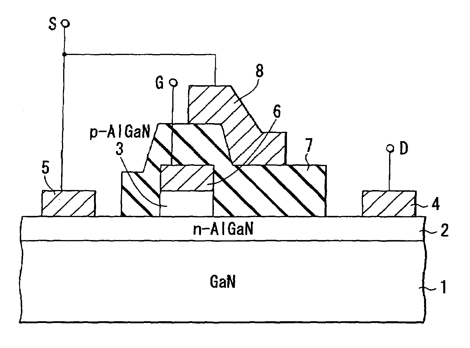
[0034]FIG. 1 is a cross-sectional view schematically showing the structure of a junction type power HEMT (High Electron Mobility Transistor) according to a first embodiment of the present invention.

[0035]The HEMT is provided with a channel layer 1 including a GaN layer (X=0) as non-dope AlXGa1-XN (0≦X≦1). The thickness of the channel layer 1 is set to about 1 to 2 μm in order to obtain a breakdown voltage of 600 V. A barrier layer 2 is formed on the surface (one side) of the channel layer 1 as n-type AlYGa1-YN (0≦Y≦1, X2 includes an Al0.2Ga0.8N layer (Y=0.2) in which Si is doped as impurity by dosage of about 1013 (atom / cm2). Further, a semiconductor layer 3 is selectively formed on the barrier layer 2 as p-type AlZGa1-ZN (0≦Z≦1) with a thickness of 0.01 μm. The semiconductor layer 3 includes an Al0.1Ga0.9N layer (Z=0.1) in which Mg is doped as impurity.

[0036]A drain electrode (D: first electrode) 4 and a source electrode (S: second electrode) 5 consisting of Ti / Al / Ni / Au are formed ...

first modification example of first embodiment

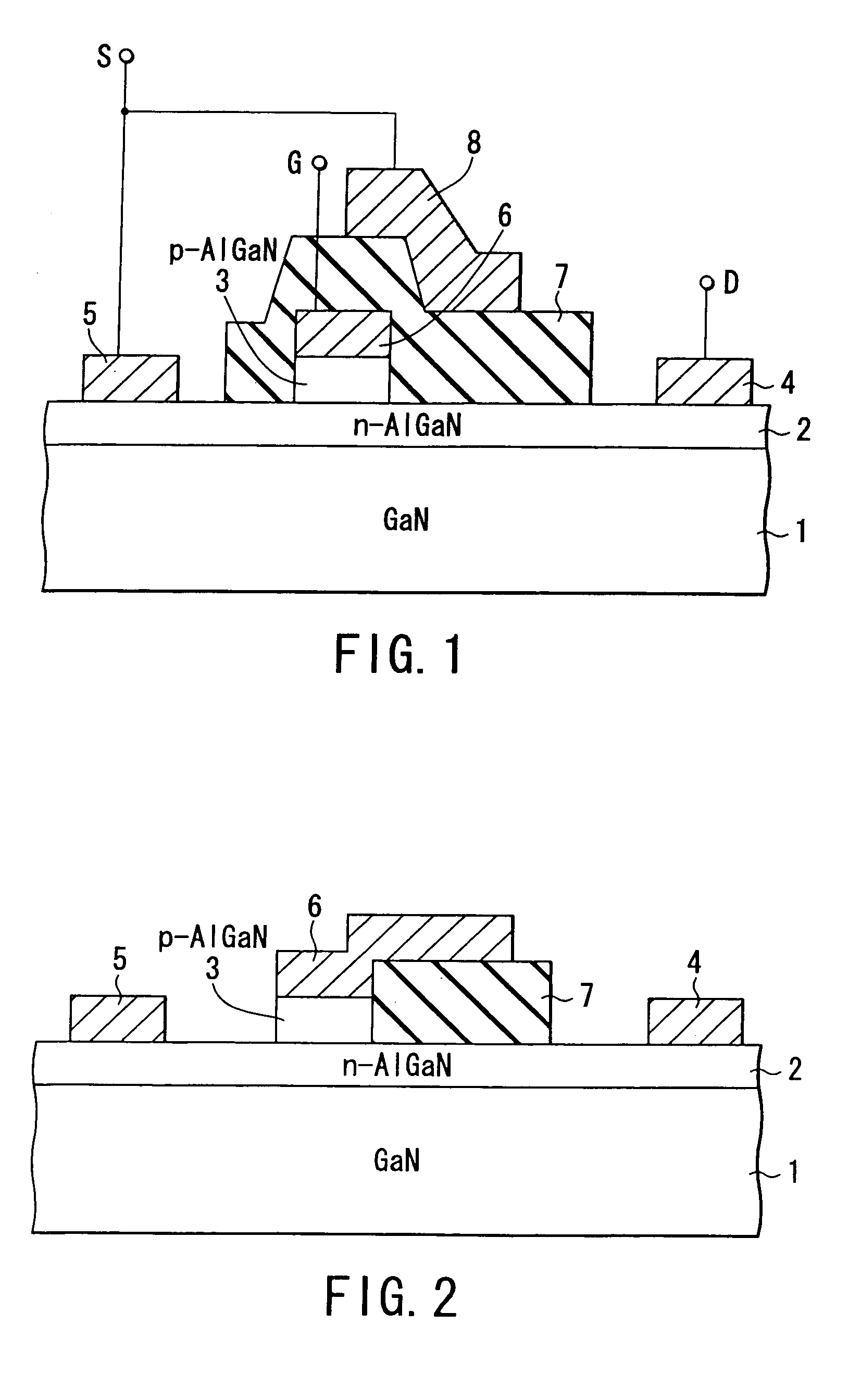
[0047]FIG. 2 is a cross-sectional view schematically showing the structure of the power HEMT shown in FIG. 1 according to a first modification example. In the power HEMT shown in FIG. 1, the dielectric layer 7 is formed so as to continuously cover the gate electrode 6 and the surrounding barrier layer 2, and the field plate electrode 8 is electrically connected to the source electrode 5.

[0048]On the contrary, the power HEMT of FIG. 2 has the following structure. That is, the dielectric layer 7 is formed so that it can be positioned between the semiconductor layer 3 and the drain electrode 4 and is adjacent to the semiconductor layer 3. The gate electrode 6 is formed so as to extend to the dielectric layer 7 in addition to the upper surface of the semiconductor layer 3. In other words, according to the first modification example, the gate electrode 6 functions concurrently as the field plate electrode 8 shown in FIG. 1.

[0049]The power HEMT of the modification example can obtain the s...

second modification example of first embodiment

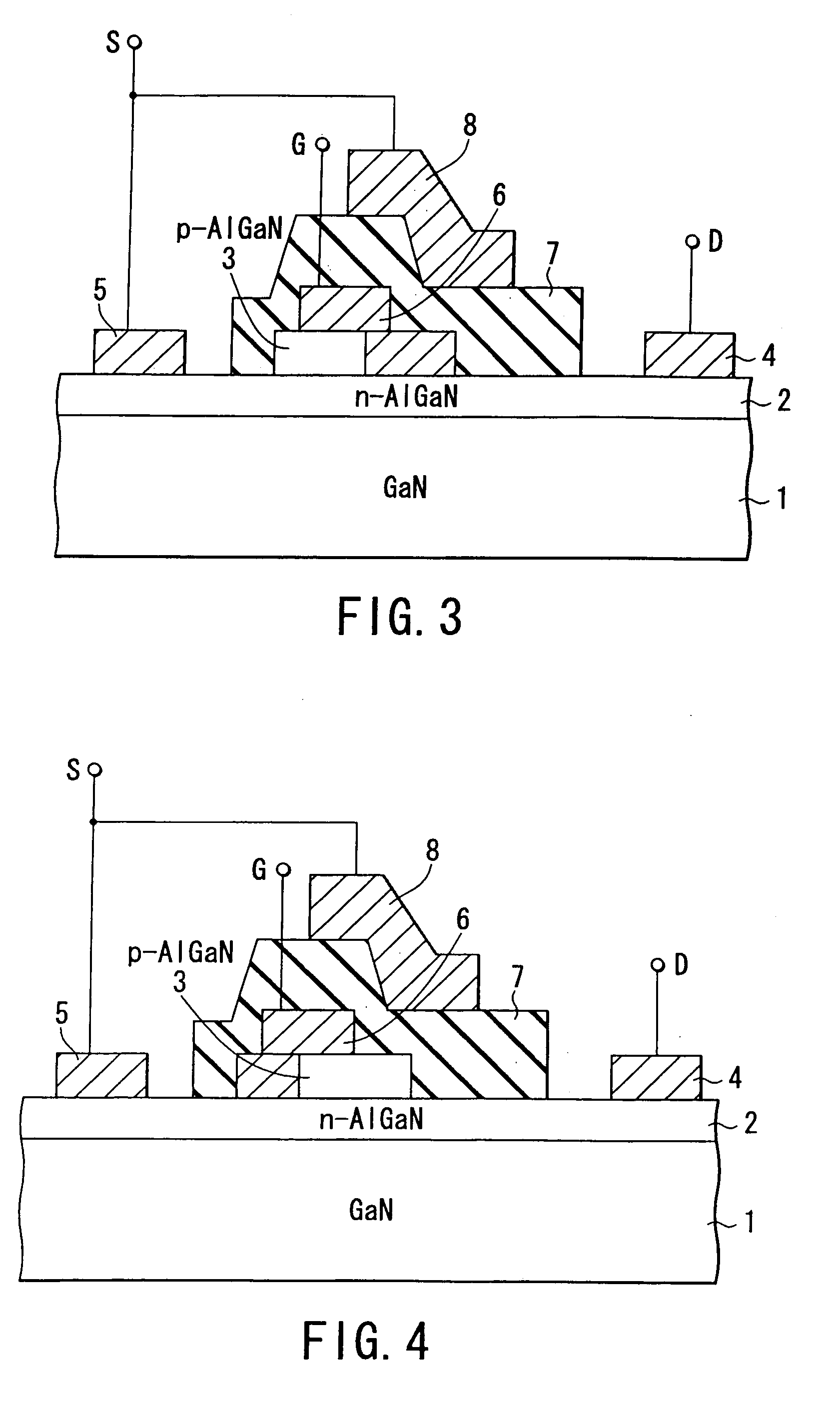
[0050]FIG. 3 is a cross-sectional view schematically showing the structure of the power HEMT shown in FIG. 1 according to a second modification example. The power HEMT of FIG. 3 differs from that of FIG. 1 in that the gate electrode 6 is formed so as to extend to the surface of the barrier layer 2 adjacent to the side of the drain electrode 4 of the semiconductor layer 3.

[0051]Namely, in the power HEMT of FIG. 3, the gate electrode 6 forms Schottky junction with the barrier layer 2.

[0052]According to the second modification example, the gate electrode 6 makes Schottky connection with the barrier layer 2. However, since the semiconductor layer 3 is connected with the gate electrode 6, holes are discharged via the semiconductor layer 3 in avalanche breakdown; therefore, high avalanche withstand capability is realized like the case of FIG. 1. Beside, the same effect as the case of FIG. 1 is obtained.


PUM


Abstract

A power semiconductor device including a non-doped GaN channel layer, an n-type Al0.2Ga0.8N barrier layer formed on the channel layer, a p-type Al0.1Ga0.9N semiconductor layer selectively formed on the barrier layer, a drain electrode positioned at one of both sides of the semiconductor layer and formed on the barrier layer, an insulating film formed on the barrier layer adjacent to the semiconductor layer between at least semiconductor layer and drain electrode, and a field plate electrode formed on the insulating film.

Description

CROSS-REFERENCE TO RELATED APPLICATIONS[0001]This is a Continuation Application of PCT Application No. PCT / JP03 / 00843, filed Jan. 29, 2003, which was published under PCT Article 21(2) in English.BACKGROUND OF THE INVENTION[0002]1. Field of the Invention[0003]The present invention relates to a power semiconductor device used for power control. In particular, the present invention relates to a lateral type power FET using nitride semiconductor, a Schottky Barrier Diode (SBD) and the like.[0004]2. Description of the Related Art[0005]Power semiconductor devices such as switching device and diode are used for power control circuits such as switching mode power supply and inverter circuit. The power semiconductor device requires the following characteristics, that is, high breakdown voltage and low ON resistance. There exists a trade-off relationship determined by device material between breakdown voltage and ON resistance in the power semiconductor device. According to recent technical a...

Claims


Application Information

Patent Timeline
Patent Type & Authority Patents(United States)
IPC IPC(8): H01L29/739H01L31/0264H01L31/0336H01L29/66H01L29/20H01L29/40H01L29/417H01L29/80H01L29/861
CPCH01L29/402H01L29/417H01L29/4175H01L29/802H01L29/861H01L29/2003
Inventor SAITO, WATARUOMURA, ICHIROOHASHI, HIROMICHI
Owner KK TOSHIBA
Why Eureka
Try Eureka