N-face high electron mobility transistors with low buffer leakage and low parasitic resistance

Inactive Publication Date: 2008-10-02
RGT UNIV OF CALIFORNIA
View PDF6 Cites 80 Cited by
  • Summary
  • Abstract
  • Description
  • Claims
  • Application Information

AI Technical Summary

Benefits of technology

[0021]The one or more N-face device layers may comprise one or more N-face first layers of (Al,Ga,In)N on the buffer layer to induce a 2DEG on top of the N-face first layers of (Al,Ga,In)N, to provide back barrier confinement for the electrons, to enhance 2DEG mobility, to increase electron velocity, and/or to provide higher breakdown voltage, and one or more N-face conductive second layers of (Al,Ga,In)N grown above the 2DEG providing lower contact or access resistances, or lower contact and access resi

Problems solved by technology

The performance of highly-scaled nitride-based HEMTs is limited by parasitic resistances at the ohmic contacts.
In Ga-face HEMTs, however, the presence of a large bandgap barrier cap, as w

Method used


Image

  • N-face high electron mobility transistors with low buffer leakage and low parasitic resistance
  • N-face high electron mobility transistors with low buffer leakage and low parasitic resistance
  • N-face high electron mobility transistors with low buffer leakage and low parasitic resistance

Examples


Embodiment Construction

[0035]In the following description of the preferred embodiment, reference is made to the accompanying drawings that form a part hereof, and in which is shown by way of illustration a specific embodiment in which the invention may be practiced. It is to be understood that other embodiments may be utilized and structural changes may be made without departing from the scope of the present invention.

[0036]Overview

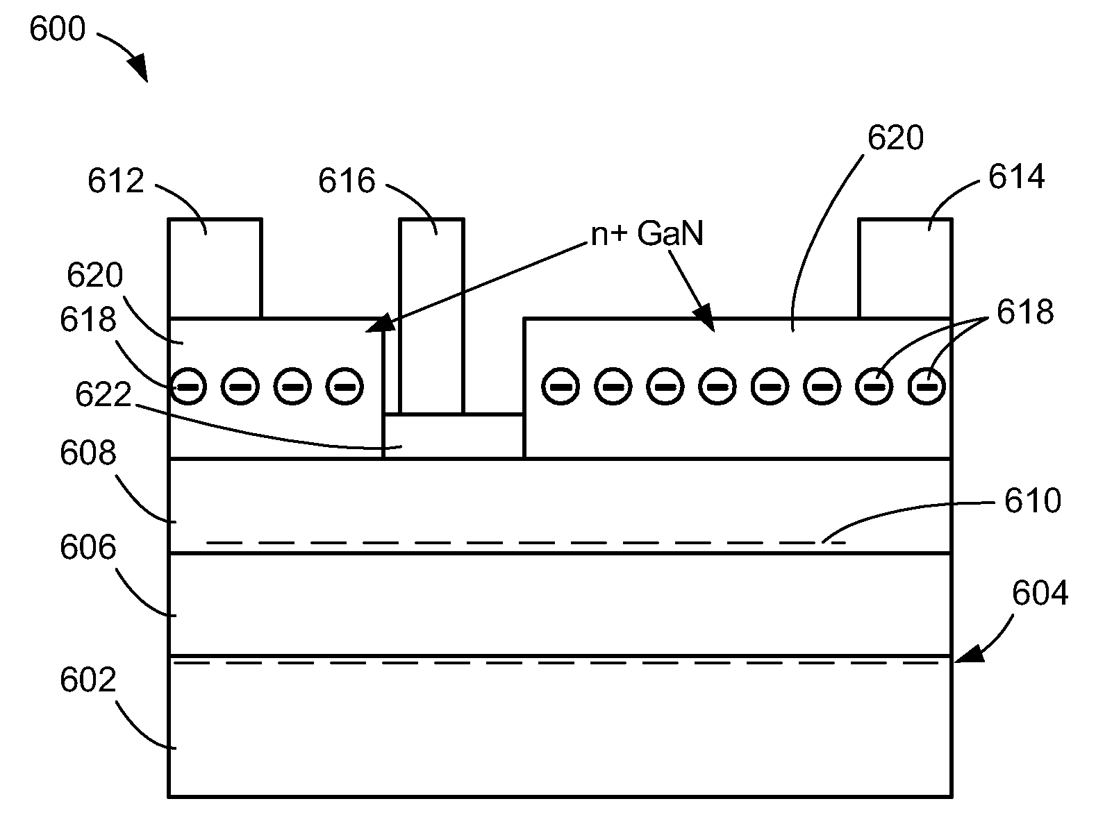
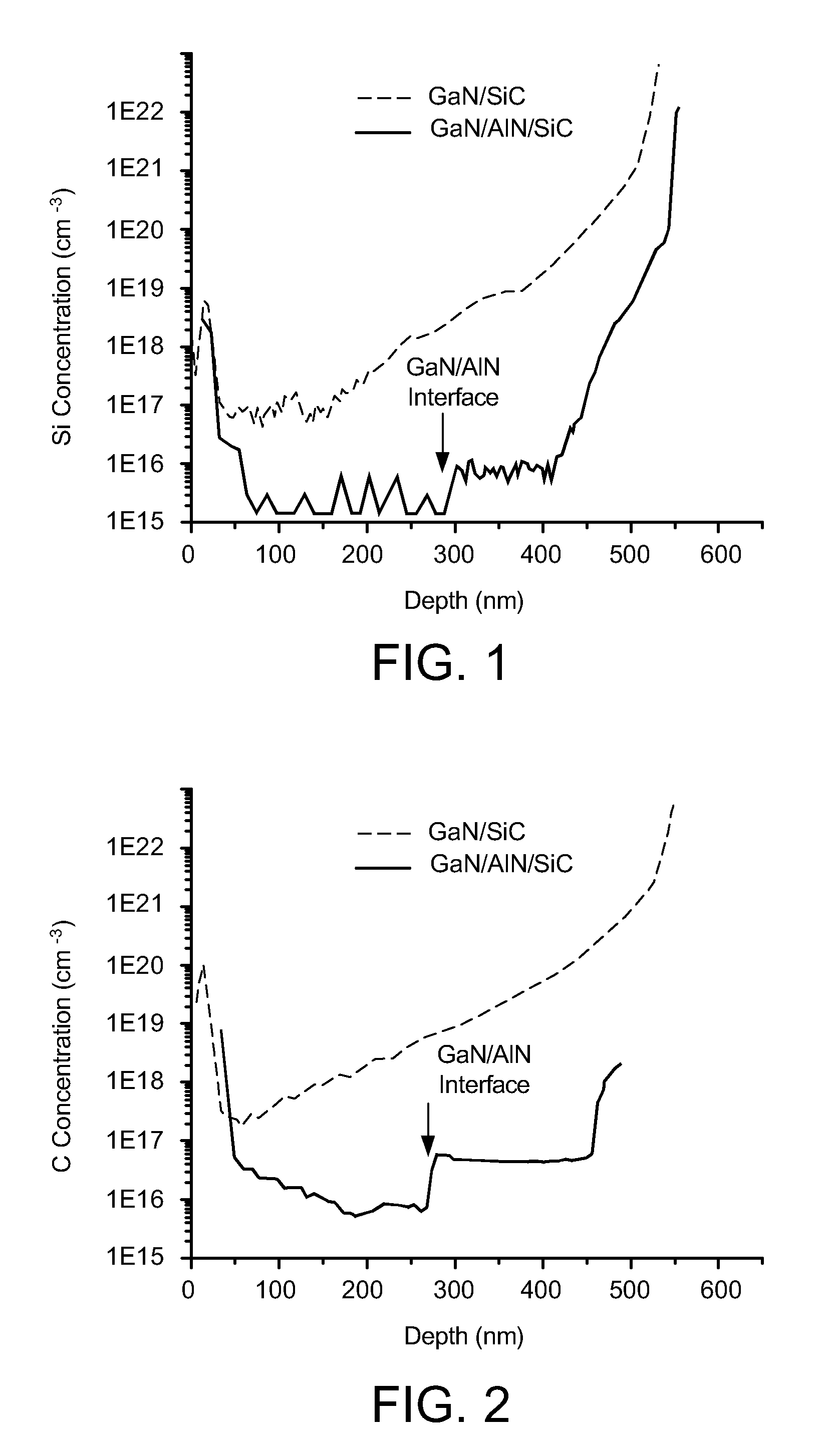
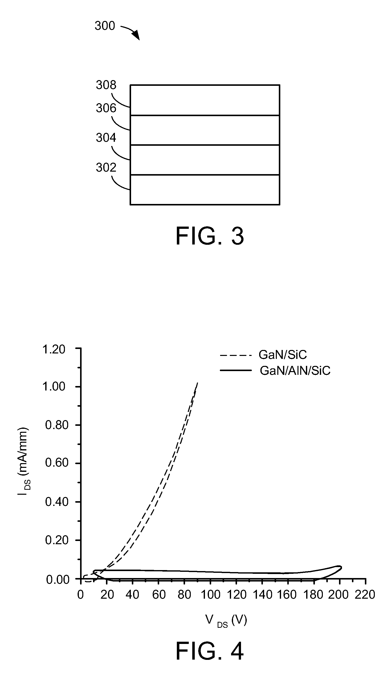
[0037]The present invention discloses new methods to fabricate N-face nitride-based electronic devices with low buffer leakage, low parasitic resistance and high breakdown. The methods comprise isolating the buffer from the substrate with an aluminum gallium indium nitride (AlGaInN) nucleation layer to suppress impurity incorporation from the substrate into the buffer, and capping the structure with a highly conductive layer to provide extremely low access and contact resistances. These new techniques offer improvements that are critical for developing mm-wave transistors with ...


PUM


Abstract

A method for fabricating nitrogen-face (N-face) nitride-based electronic devices with low buffer leakage, comprising isolating a buffer from a substrate with an AlGaInN nucleation layer to suppress impurity incorporation from the substrate into the buffer. A method for fabricating N-face nitride-based electronic devices with low parasitic resistance and high breakdown, comprising capping a device structure with a conductive layer to provide extremely low access and/or contact resistances, is also disclosed.

Description

CROSS-REFERENCE TO RELATED APPLICATIONS[0001]This application claims the benefit under 35 U.S.C. Section 119(e) of the following co-pending and commonly-assigned U.S. patent application:[0002]U.S. Provisional Patent Application Ser. No. 60 / 908,914, filed on Mar. 29, 2007, by Umesh K. Mishra, Yi Pei, Siddharth Rajan, and Man Hoi Wong, entitled “N-FACE HIGH ELECTRON MOBILITY TRANSISTORS WITH LOW BUFFER LEAKAGE AND LOW PARASITIC RESISTANCE,” attorneys docket number 30794.215-US-P1 (2007-269);[0003]which application is incorporated by reference herein.[0004]This application is related to the following co-pending and commonly assigned application:[0005]U.S. Utility patent application Ser. No. ______, filed on same date herewith, by Umesh K. Mishra, Lee S. McCarthy, Chang Soo Suh and Siddharth Rajan, entitled “METHOD TO FABRICATE III-N SEMICONDUCTOR DEVICES ON THE N-FACE OF LAYERS WHICH ARE GROWN IN THE III-FACE DIRECTION USING WAFER BONDING AND SUBSTRATE REMOVAL”, attorney's docket numbe...

Claims


Application Information

Patent Timeline
IPC IPC(8): H01L29/267H01L21/205H01L21/336
CPCH01L21/02378H01L21/02433H01L21/02458H01L21/02516H01L21/0254H01L29/0891H01L29/1608H01L29/2003H01L29/7786
Inventor MISHRA, UMESH K.PEI, YIRAJAN, SIDDHARTHWONG, MAN HOI
Owner RGT UNIV OF CALIFORNIA
Why Eureka
Try Eureka