
High electron mobility transistor

a high-electromagnetic transistor and electron mobility technology, applied in transistors, semiconductor devices, electrical apparatus, etc., can solve the problems of poor linearity characteristics, sharp peak in transconductance, and devices suffering from significantly reduced electron mobility, and achieve superior linearity and electron mobility characteristics.

Active Publication Date: 2007-08-07
WOLFSPEED INC
View PDF10 Cites 79 Cited by
  • Summary
  • Abstract
  • Description
  • Claims
  • Application Information

AI Technical Summary

Benefits of technology

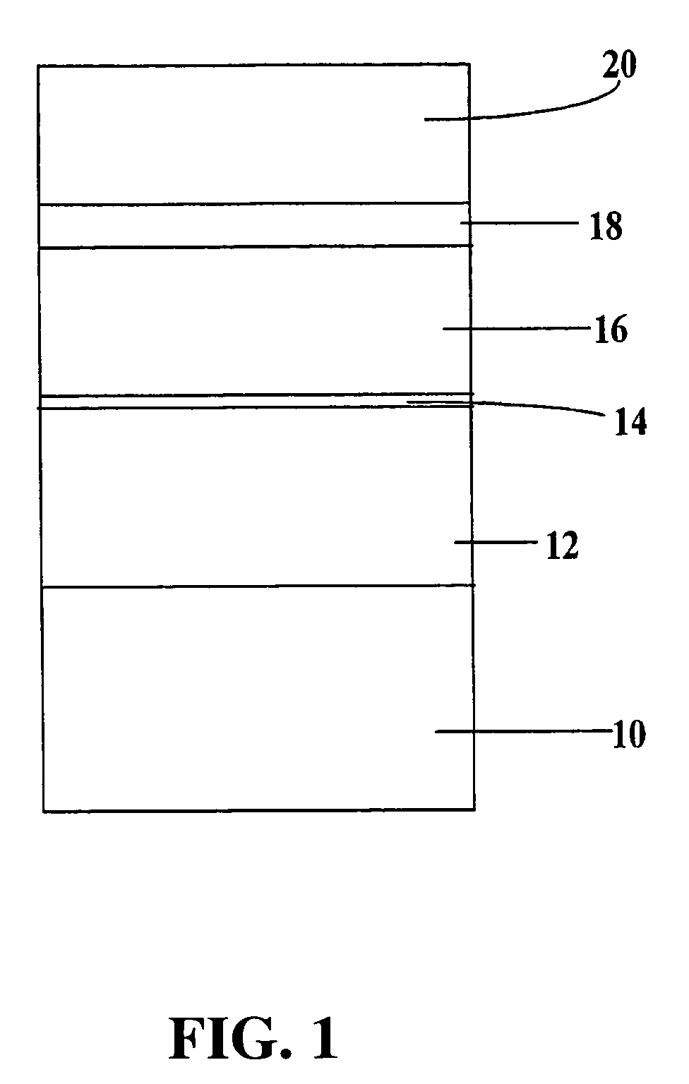
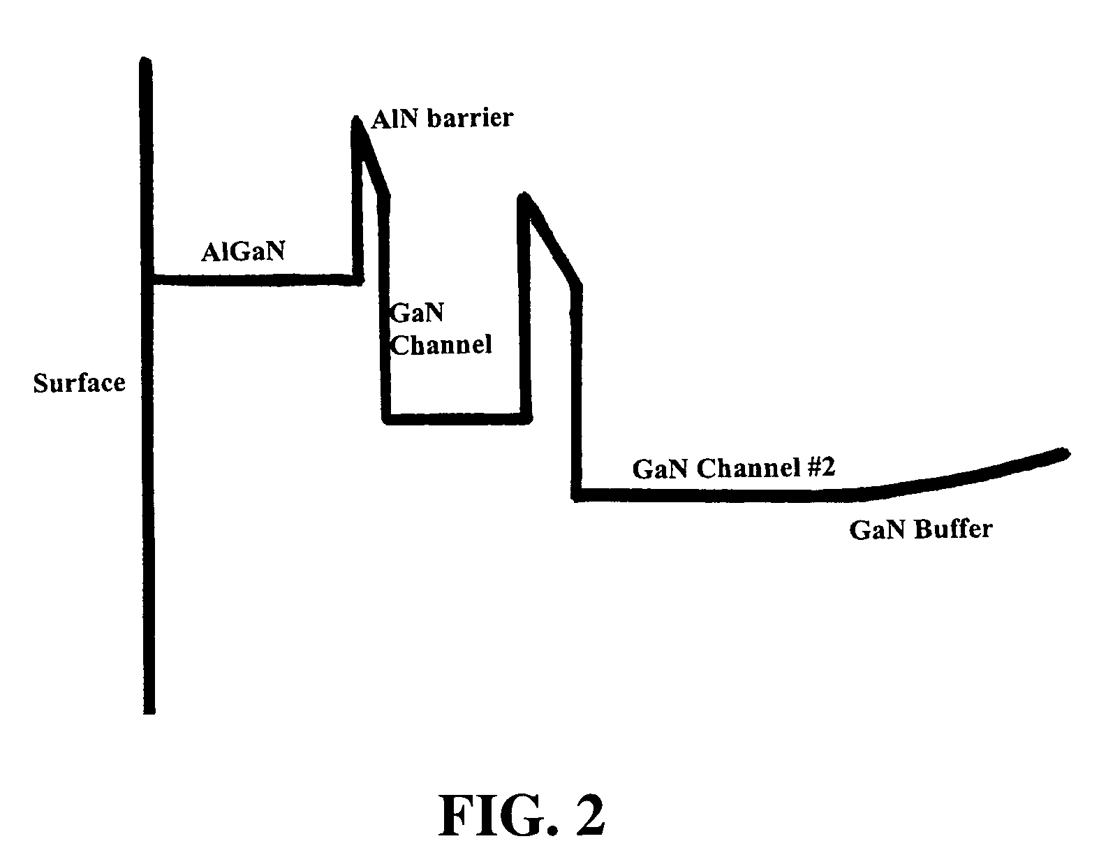
The invention is about a new type of HEMT device that includes a very thin layer made of a nitride composition between two layers of GaN. This layer helps to bend the electric field and spread the charge carriers (electrons) throughout the device, which improves its performance and makes it more linear. The device can be used in high-speed applications like DHFETs. The invention also includes a method for improving the linearity of the device without sacrificing its electron mobility.

Problems solved by technology

Conventional HEMTs have a narrow peak in the distribution of electrons as a function of depth, which results in a sharp peak in transconductance and poor linearity characteristics.
Unfortunately, such devices suffer from significantly reduced electron mobility, since the two-dimensional electron gas (2DEG) is predominately contained within the AlGaN alloy and alloy scattering of the electrons is a significant effect.

Method used


Image

  • High electron mobility transistor
  • High electron mobility transistor
  • High electron mobility transistor

Examples


examples

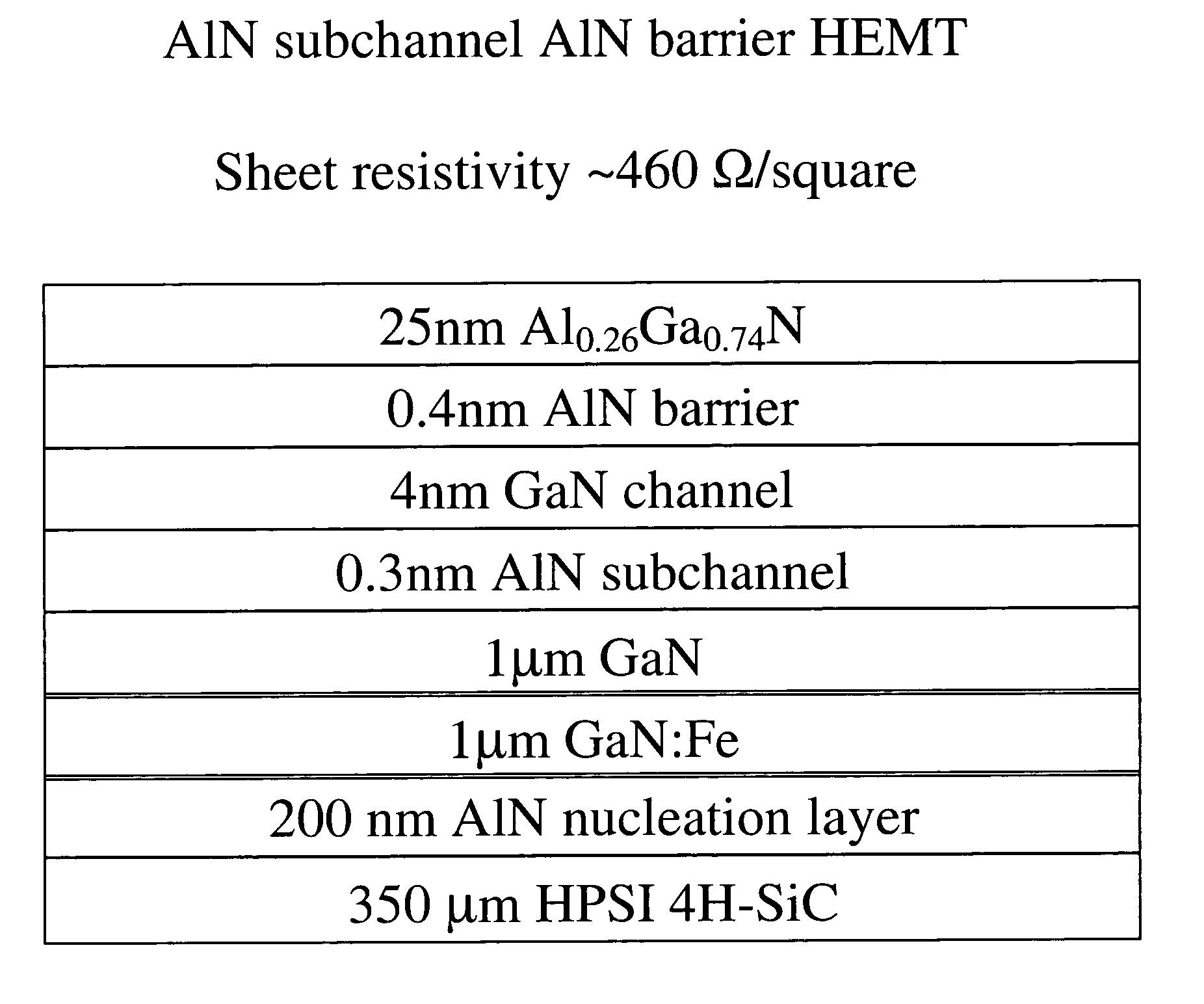
[0070]Referring now to the further drawings FIGS. 10–12, FIG. 10 is a schematic representation of a HEMT device structure including an AlN barrier layer and characterized by a sheet mobility of ˜330 Ω / square, FIG. 11 is a schematic representation of a HEMT device structure including an AlGaN channel and an AlN barrier layer and characterized by a sheet mobility of ˜610 Ω / square, and FIG. 12 is a schematic representation of a HEMT device structure including an AlN subchannel and an AlN barrier layer and characterized by a sheet mobility of ˜460 Ω / square.

[0071]In each of FIGS. 10–12, the thicknesses of the respective layers in the device structure are set out in appropriate dimensional units of microns (μm) or nanometers (nm).

[0072]Each of the AlN barrier HEMT structures in FIGS. 10–12 was grown under substantially the same growth conditions as the others. All epitaxial III-Nitride layers were deposited by low pressure MOCVD (metalorganic chemical vapor deposition). Precursors used we...


PUM


Abstract

A HEMT device including a GaN channel structure including a very thin (Al,In,Ga)N subchannel layer that is disposed between a first GaN channel layer and a second GaN channel layer, to effect band bending induced from the piezoelectric and spontaneous charges associated with the (Al,In,Ga)N subchannel layer. This GaN channel / (Al,In,Ga)N subchannel arrangement effectively disperses the 2DEG throughout the channel of the device, thereby rendering the device more linear in character (relative to a corresponding device lacking the subchannel (Al,In,Ga)N sub-layer), without substantial loss of electron mobility.

Description

FIELD OF THE INVENTION[0001]The present invention relates to a high electron mobility transistor (HEMT) device.DESCRIPTION OF THE RELATED ART [0002]Gallium nitride (GaN) and GaN-based materials have physical and electronic properties that make them attractive for high temperature, high power and high frequency microelectronic devices. These properties include wide bandgap character, low thermal carrier generation rates, high breakdown field, high electron mobility and high electron velocity.[0003]These properties of GaN and GaN-based materials render them advantageous for use in high electron mobility transistor devices, characterized by high electron mobilities, superior charge confinement and high breakdown voltage. Room temperature radio frequency (2–10 GHz) output power >2 W / mm is enabled by such GaN and GaN-based materials.[0004]Conventional HEMTs have a narrow peak in the distribution of electrons as a function of depth, which results in a sharp peak in transconductance and...

Claims


Application Information

Patent Timeline
Patent Type & Authority Patents(United States)
IPC IPC(8): H01L31/00
CPCH01L29/1029H01L29/7787H01L29/2003
Inventor SAXLER, ADAM WILLIAM
Owner WOLFSPEED INC
Learn More