

High electron mobility transistor
- Summary
- Abstract
- Description
- Claims
- Application Information
AI Technical Summary
Benefits of technology
Problems solved by technology
Method used
Image

Examples
examples
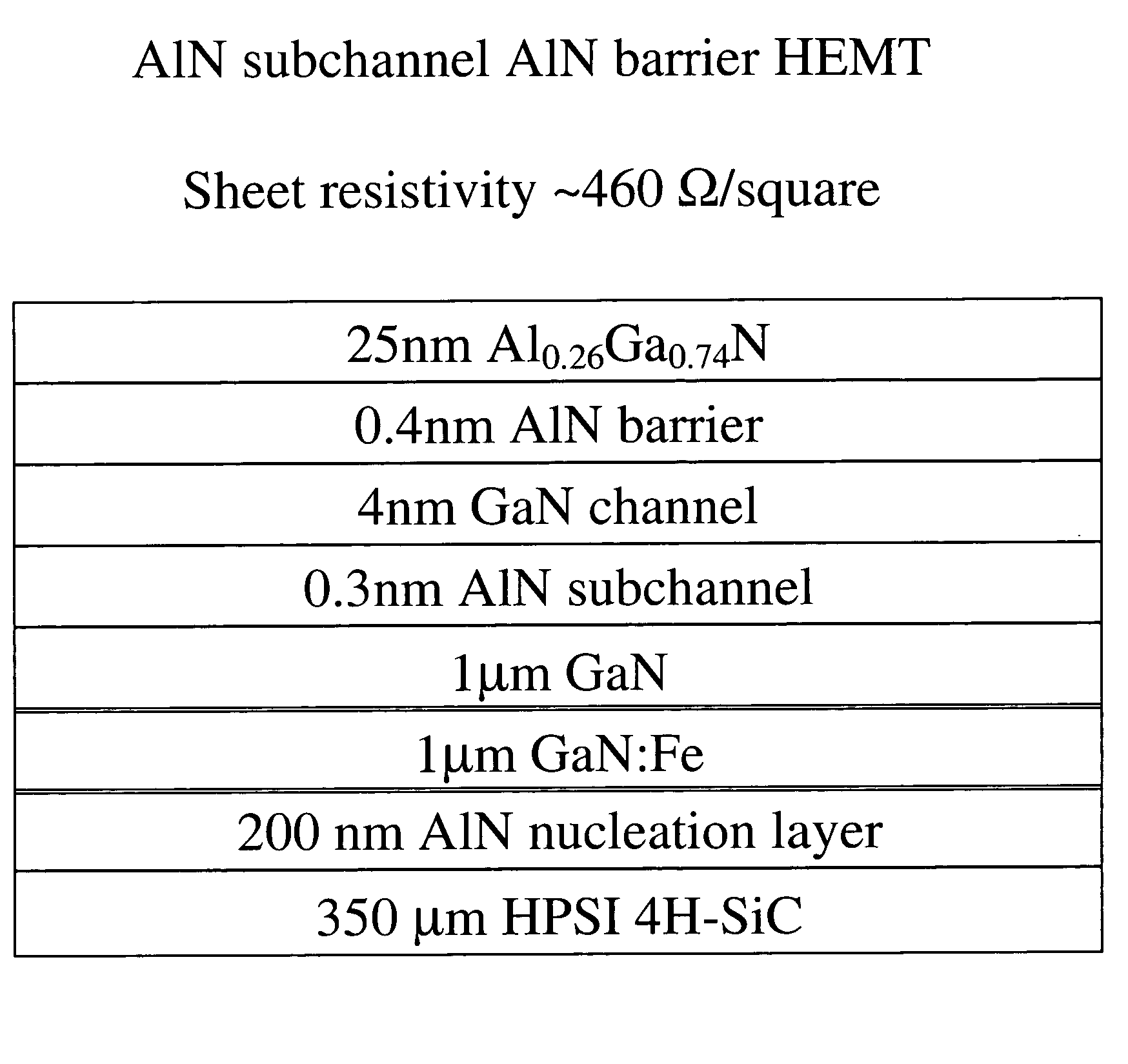
[0070] Referring now to the further drawings FIGS. 10-12, FIG. 10 is a schematic representation of a HEMT device structure including an AlN barrier layer and characterized by a sheet mobility of ˜330 Ω / square, FIG. 11 is a schematic representation of a HEMT device structure including an AlGaN channel and an AlN barrier layer and characterized by a sheet mobility of ˜610 Ω / square, and FIG. 12 is a schematic representation of a HEMT device structure including an AlN subchannel and an AlN barrier layer and characterized by a sheet mobility of ˜460 Ω / square.
[0071] In each of FIGS. 10-12, the thicknesses of the respective layers in the device structure are set out in appropriate dimensional units of microns (μm) or nanometers (nm).
[0072] Each of the AlN barrier HEMT structures in FIGS. 10-12 was grown under substantially the same growth conditions as the others. All epitaxial III-Nitride layers were deposited by low pressure MOCVD (metalorganic chemical vapor deposition). Precursors us...
PUM
 Abstract
Description
Claims
Application Information