P-GaN/AlGaN/AlN/GaN enhancement-mode field effect transistor

a field effect transistor and enhancement mode technology, applied in the field of enhancement mode field effect transistors, can solve the problems of low resistance, and achieve the effect of high electron mobility transistors, low resistance, and high gate turn-on

Active Publication Date: 2010-06-01
RGT UNIV OF CALIFORNIA
View PDF3 Cites 79 Cited by
  • Summary
  • Abstract
  • Description
  • Claims
  • Application Information

AI Technical Summary

Benefits of technology

[0018]To overcome the limitations in the prior art described above, and to overcome other limitations that will become apparent upon reading and understanding the present specification, the present invention discloses a novel enhancement mode High Electron Mobility Transistor (HEMT) structure with a p-GaN cap layer for high gate turn-on plus an aluminum nitride (AlN) interlayer for low on-resistance.
[0019]Under the gate, this transistor has a p-GaN / AlGaN / AlN / GaN epilayer structure. The high barrier of the p-GaN layer depletes the electron gas at the AlN / GaN interface under zero gate bias, and also increases the gate turn-on voltage. Furthermore, changing the aluminum (Al) composition and the thickness of the AlGaN layer controls the threshold voltage over a wide range.
[0021]The present invention discloses a method for fabricating a field effect transistor, comprising using a III-nitride barrier layer to control a threshold voltage of a gate of the transistor and confine a two dimensional electron gas (2DEG) to a channel layer of the transistor; and using a polarization induced electric field of a III-nitride interlayer between the 2DEG and the III-nitride barrier layer to induce a larger 2DEG charge density as compared to without the III-nitride interlayer, thereby reducing an on-resistance of the transistor and controlling the on-resistance independently of the threshold voltage.

Problems solved by technology

Without the high barrier of p-GaN, polarization fields in the AlGaN and AlN layers allow a charge sheet to form at the AlN / GaN interface, thus leading to low on-resistance.

Method used


Image

  • P-GaN/AlGaN/AlN/GaN enhancement-mode field effect transistor
  • P-GaN/AlGaN/AlN/GaN enhancement-mode field effect transistor
  • P-GaN/AlGaN/AlN/GaN enhancement-mode field effect transistor

Examples


Embodiment Construction

[0052]In the following description of the preferred embodiment, reference is made to the accompanying drawings which form a part hereof, and in which is shown by way of illustration a specific embodiment in which the invention may be practiced. It is to be understood that other embodiments may be utilized and structural changes may be made without departing from the scope of the present invention.

[0053]Technical Description

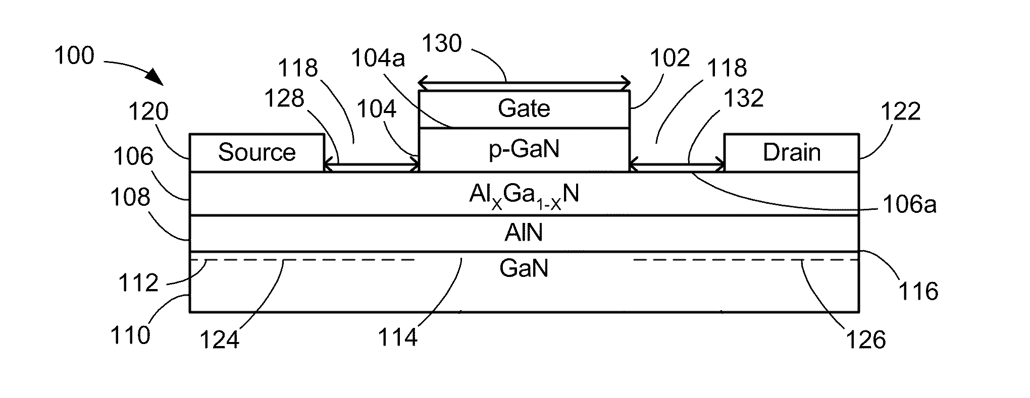
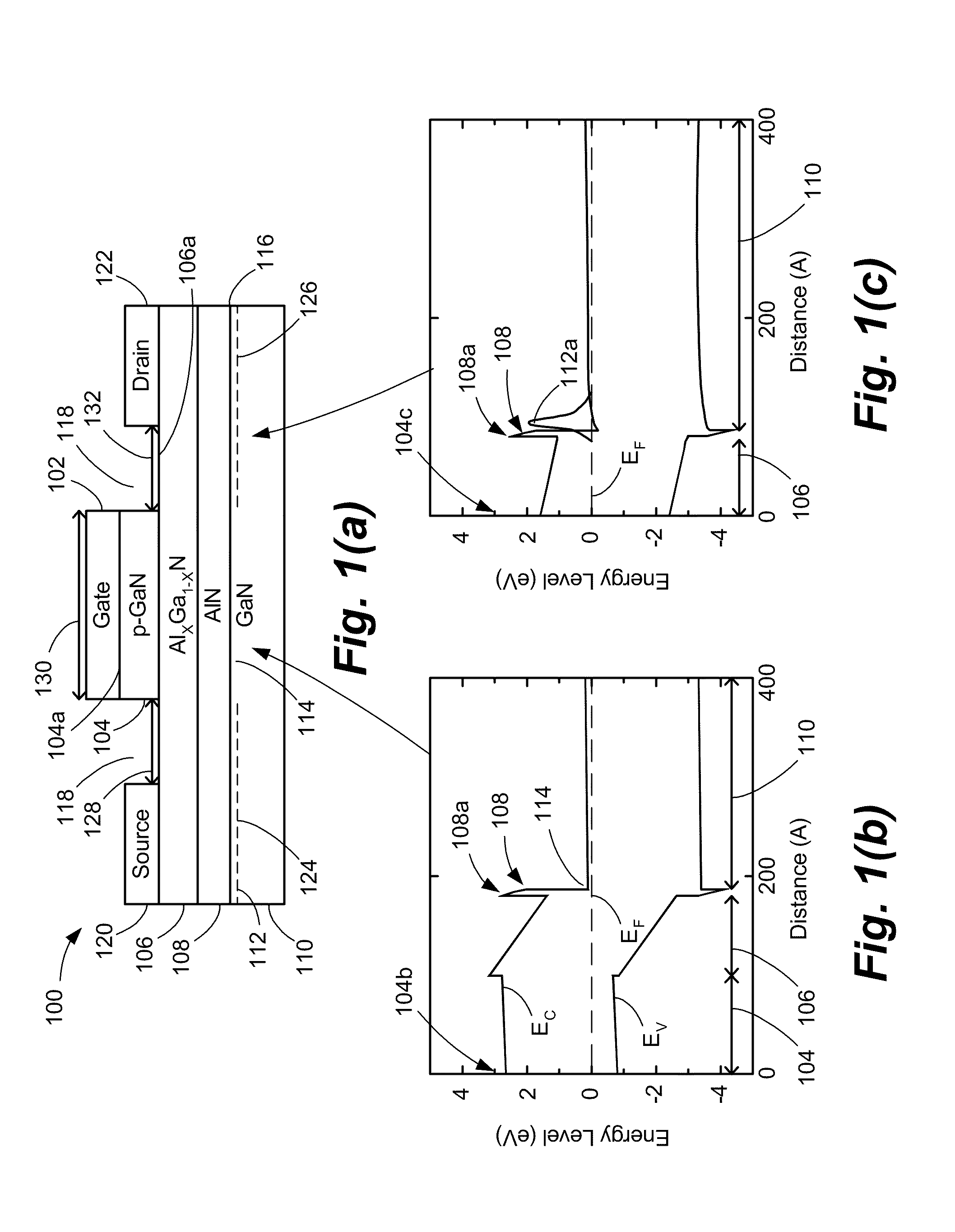
[0054]The present invention comprises a device structure with a p-GaN cap layer and an AlN interlayer which does not have the drawbacks seen in the above mentioned devices. The structure for this device 100 is shown in FIG. 1(a). Under the gate 102, the epilayer stack comprises (from top to bottom) p-GaN 104, AlxGal1-xN 106 (with 0108 and a GaN-buffer 110. The high barrier of the p-GaN104 layer fully depletes the electron gas 112 at the portion 114 of the interface 116 (between the AlN 108 and GaN-buffer 110) which is under the gate 102 (under zero gate bias, see ...


PUM


Abstract

An enhancement mode High Electron Mobility Transistor (HEMT) comprising a p-type nitride layer between the gate and a channel of the HEMT, for reducing an electron population under the gate. The HEMT may also comprise an Aluminum Nitride (AlN) layer between an AlGaN layer and buffer layer of the HEMT to reduce an on resistance of a channel.

Description

CROSS-REFERENCE TO RELATED APPLICATIONS[0001]This application claims the benefit under 35 U.S.C. Section 119(e) of commonly-assigned U.S. Provisional Patent Application Ser. No. 60 / 941,580 filed on Jun. 1, 2007, by Chang Soo Suh and Umesh K. Mishra, entitled “P-GaN / AlGaN / AlN / GaN ENHANCEMENT-MODE FIELD EFFECT TRANSISTOR”, which application is incorporated by reference herein.[0002]This application is related to the following co-pending and commonly-assigned applications:[0003]U.S. Utility patent application Ser. No. 10 / 962,911, filed on Oct. 12, 2004, by Likun Shen, Sten J. Heikman and Umesh K. Mishra, entitled “GaN / AlGaN / GaN DISPERSION-FREE HIGH ELECTRON MOBILITY TRANSISTORS,”, which application claims the benefit under 35 U.S.C Section 119(e) of U.S. Provisional Application Ser. No. 60 / 510,695, filed on Oct. 10, 2003, by Likun Shen, Sten J. Heikman and Umesh K. Mishra, entitled “GaN / AlGaN / GaN DISPERSION-FREE HIGH ELECTRON MOBILITY TRANSISTORS,”;[0004]U.S. patent application Ser. No...

Claims


Application Information

Patent Timeline
Patent Type & Authority Patents(United States)
IPC IPC(8): H01L29/778
CPCH01L29/1066H01L29/2003H01L29/7786H01L29/432H01L29/66462H01L29/42316
Inventor SUH, CHANG SOOMISHRA, UMESH K.
Owner RGT UNIV OF CALIFORNIA
Why Eureka
Try Eureka