

High mobility monolithic p-i-n diodes
- Summary
- Abstract
- Description
- Claims
- Application Information
AI Technical Summary
Benefits of technology
Problems solved by technology
Method used
Image

Examples
Embodiment Construction
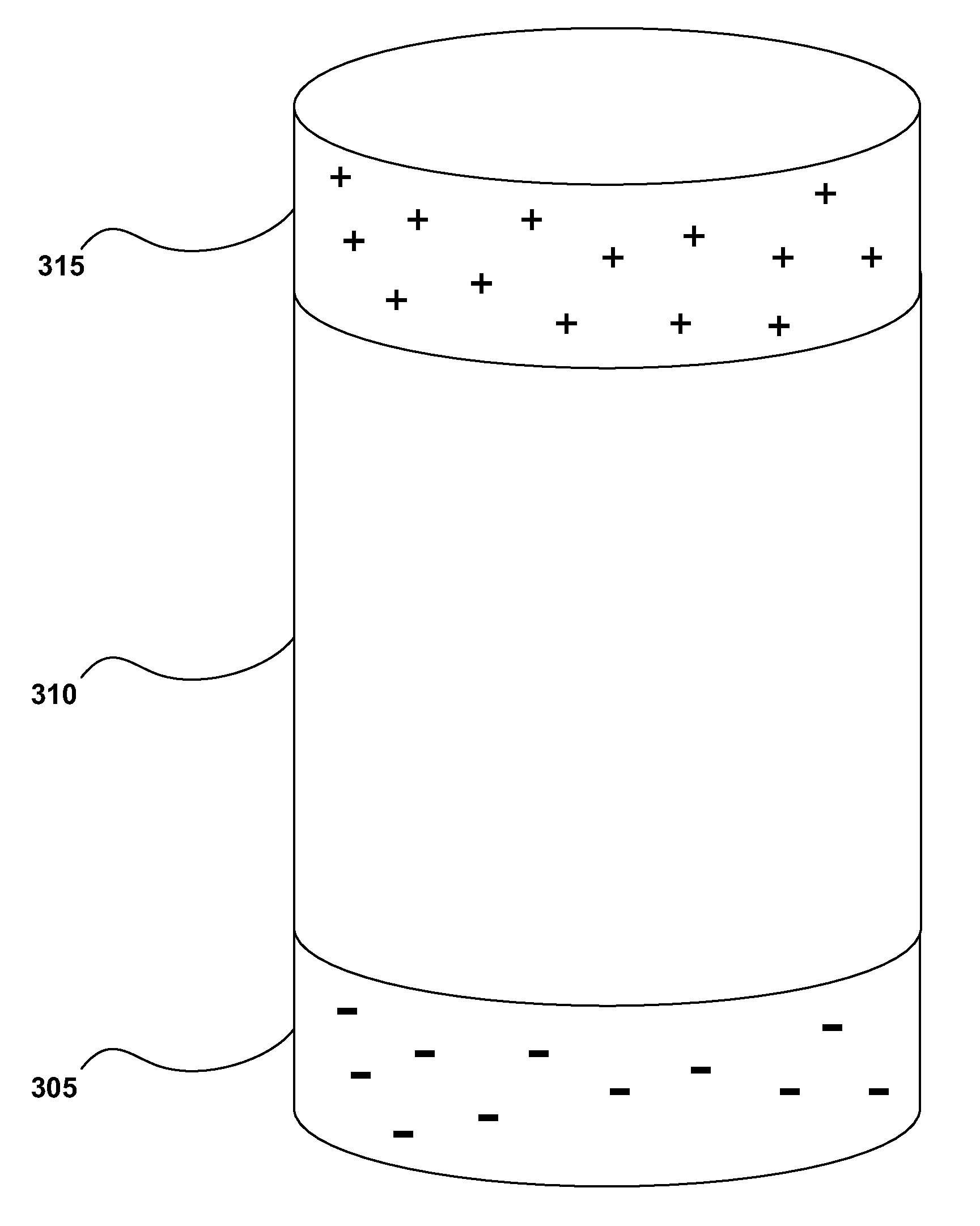
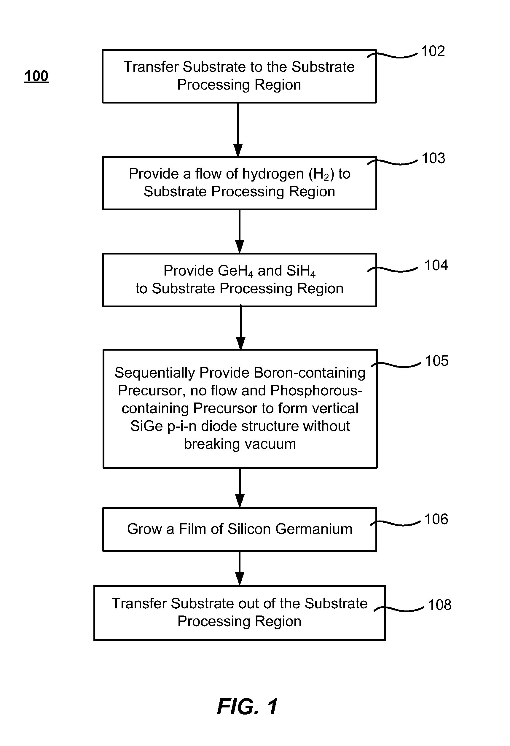
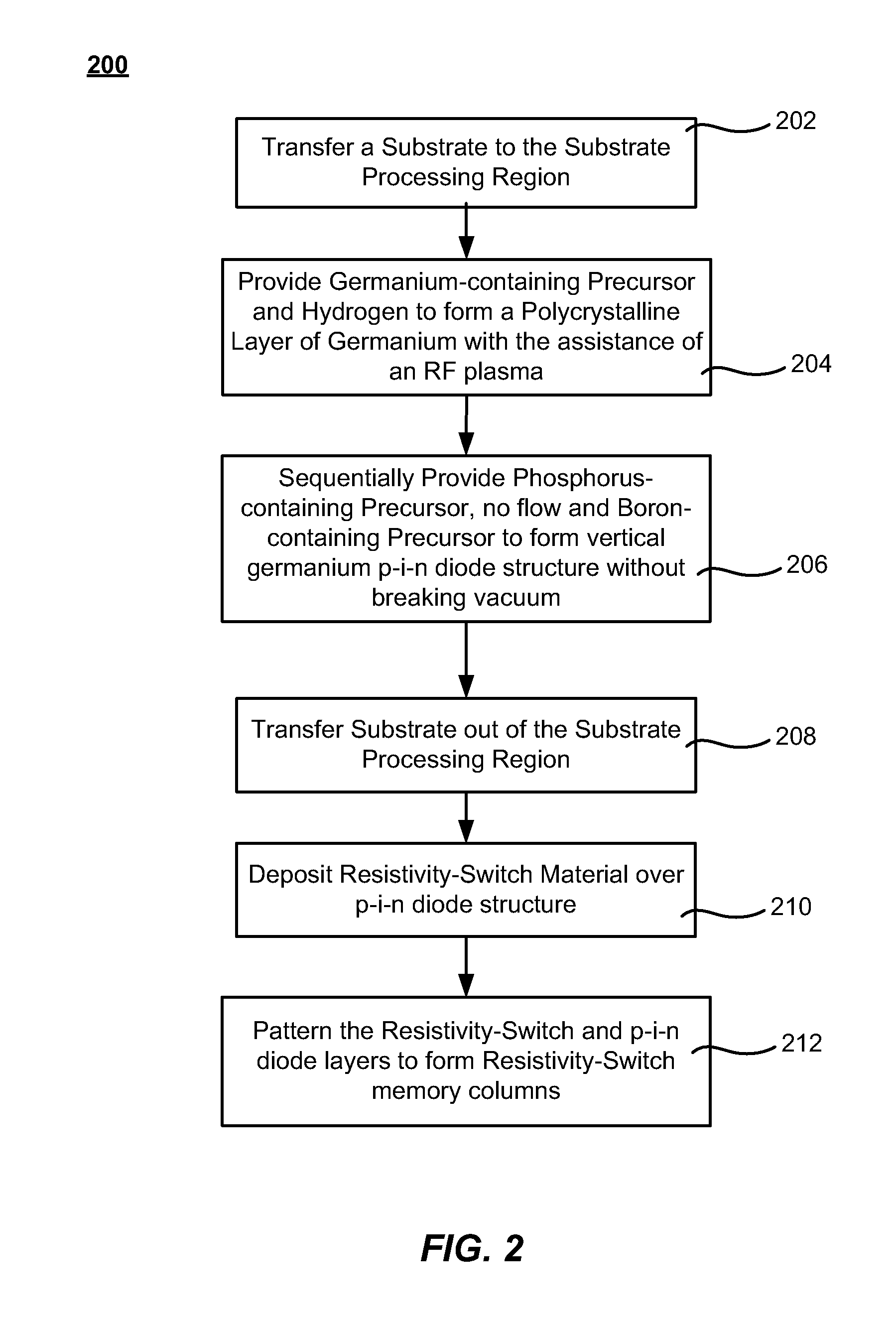
[0014]Methods of forming high-current density vertical p-i-n diodes on a substrate are described. The methods include the steps of concurrently combining a group-IV-element-containing precursor with a sequential exposure to an n-type dopant precursor and a p-type dopant precursor in either order. An intrinsic layer is deposited between the n-type and p-type layers by reducing or eliminating the flow of the dopant precursors while flowing the group-IV-element-containing precursor. The substrate may reside in the same processing chamber during the deposition of each of the n-type layer, intrinsic layer and p-type layer and the substrate is not exposed to atmosphere between the depositions of adjacent layers.
[0015]The methods presented herein allow a p-i-n diode stack to be formed without the use of ion implantation which would necessitate a high temperature anneal to activate the implanted dopants. The p-i-n diode stack is also formed without exposing the substrate to the atmosphere d...
PUM
| Property | Measurement | Unit |
|---|---|---|
| Width | aaaaa | aaaaa |
| Area | aaaaa | aaaaa |
| Flow rate | aaaaa | aaaaa |
Abstract
Description
Claims
Application Information