Methods and Systems for Chip-to-Chip Communication with Reduced Simultaneous Switching Noise

a technology of simultaneous switching and communication method, applied in the direction of transmission, instruments, electric digital data processing, etc., can solve the problems of simultaneous switching output noise or sso, anomalous noise, undesirable secondary effects of signaling using a plurality of wires that change state simultaneously, etc., to achieve no or reduced simultaneous switching output noise, high speed, and low latency interface

Active Publication Date: 2015-12-31
KANDOU LABS
View PDF2 Cites 41 Cited by
  • Summary
  • Abstract
  • Description
  • Claims
  • Application Information

AI Technical Summary

Benefits of technology

This patent describes methods and devices that allow for transmitting data over physical channels to create a fast and low-latency interface. Compared to single-ended interfaces, this technology reduces the noise caused by simultaneous switching.

Problems solved by technology

Signaling using a plurality of wires that change state simultaneously may be associated with undesirable secondary effects within the output circuit, due to the physical need to change the output level on multiple wire loads.
The resulting anomalous noise, caused by this current draw from power sources and / or current drain into ground lines and / or power returns, is known as Simultaneous Switched Output noise or SSO.

Method used


Image

  • Methods and Systems for Chip-to-Chip Communication with Reduced Simultaneous Switching Noise
  • Methods and Systems for Chip-to-Chip Communication with Reduced Simultaneous Switching Noise
  • Methods and Systems for Chip-to-Chip Communication with Reduced Simultaneous Switching Noise

Examples


Embodiment Construction

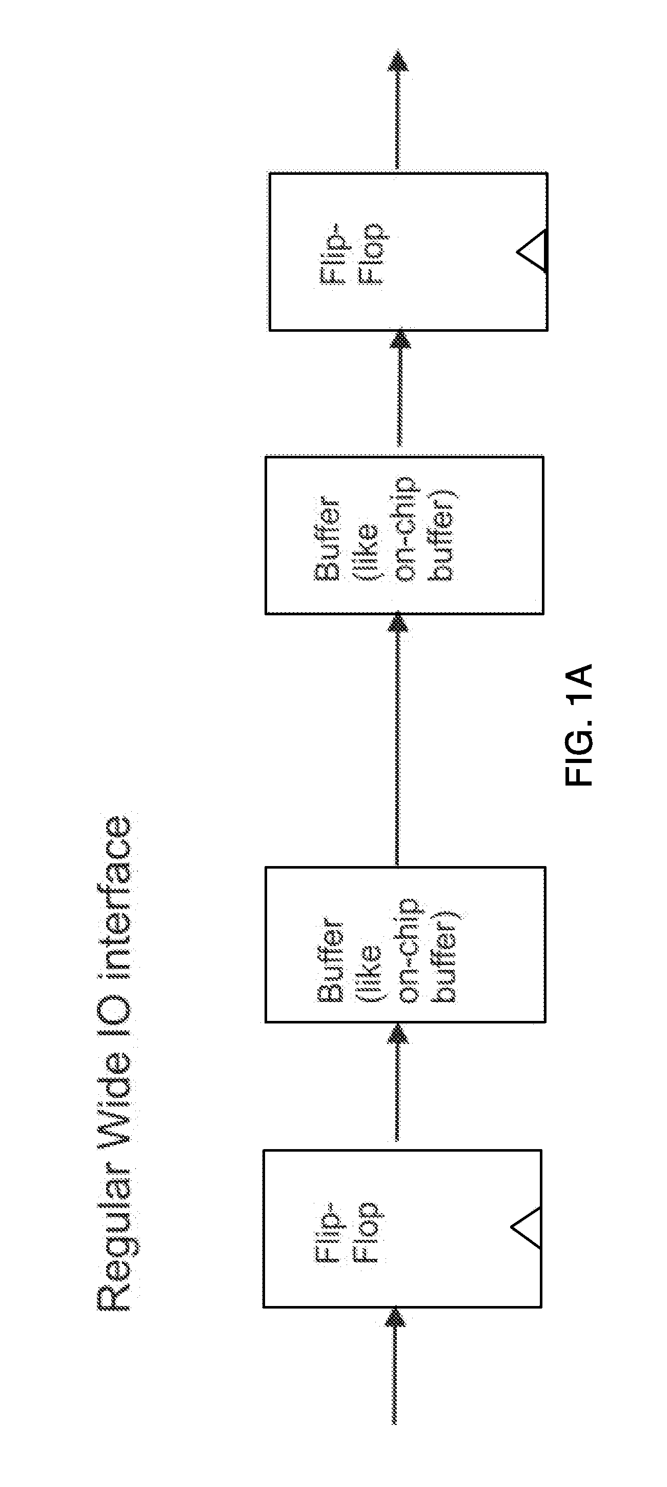
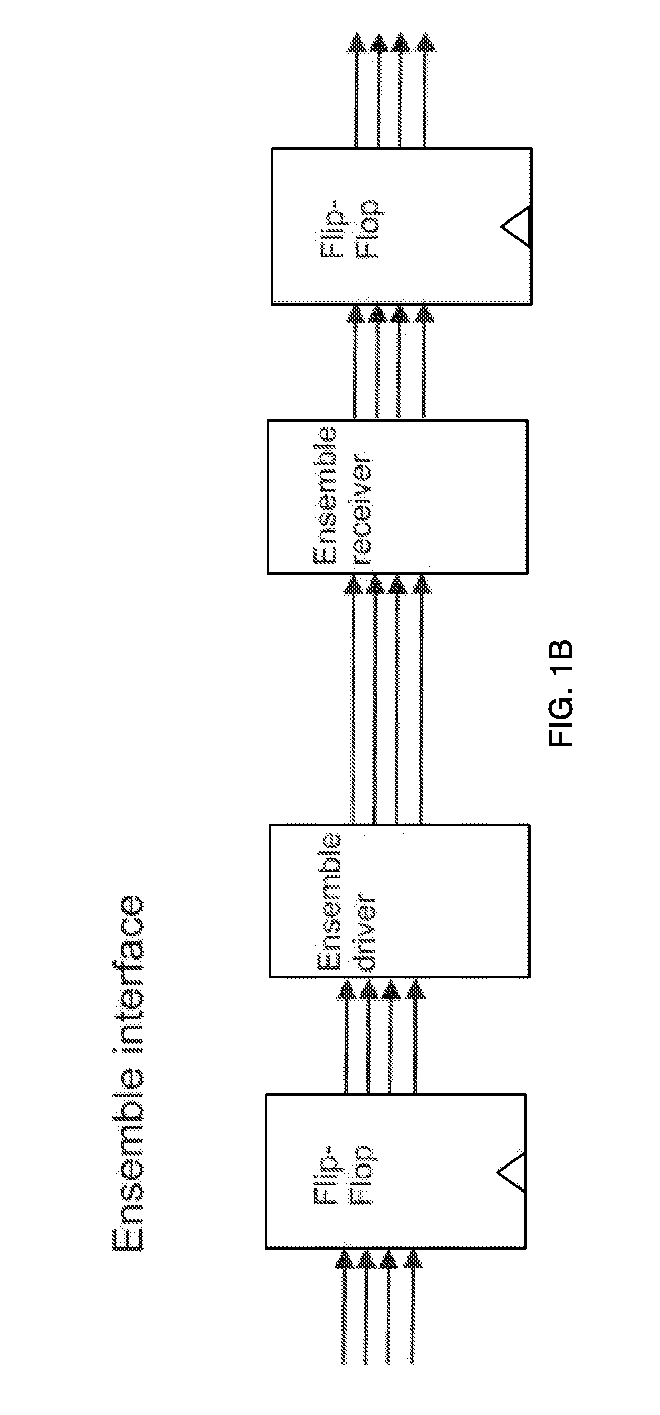
[0028]Specialized memory subsystems of modern computer systems utilize dedicated memory controllers to manage access, optimize performance, and improve utilization and reliability. Interconnections between these memory controllers and memory devices must operate at high speeds, delivering reliable and low latency data transfers, while under significant constraints in terms of available pin count and power utilization. To maximize data transfer throughput and efficiency, extremely wide data transfer operations are the norm, typically of 128 bits or more per cycle, as shown in the block diagram of FIG. 1A. These wide I / O transfers put considerable strain on output driver power utilization, especially when many bits change state simultaneously. Such Simultaneous Switched Output transitions may draw significant power supply current and / or introduce considerable return current into the ground line, significantly raising the system noise level.

[0029]Methods of addressing Simultaneous Swit...


PUM


Abstract

Systems and methods are described for transmitting data over physical channels to provide a high speed, low latency interface such as between a memory controller and memory devices with significantly reduced or eliminated Simultaneous Switching Output noise. Controller-side and memory-side embodiments of such channel interfaces are disclosed which do not require additional pin count or data transfer cycles, have low power utilization, and introduce minimal additional latency. In some embodiments of the invention, three or more voltage levels are used for signaling.

Description

CROSS REFERENCE TO RELATED APPLICATIONS[0001]This application is a continuation of U.S. application Ser. No. 14 / 158,452, filed Jan. 17, 2014, naming John Fox, entitled “Methods and Systems for Chip-to-Chip Communication with Reduced Simultaneous Switching Noise, which is a non-provisional application claiming priority to U.S. provisional application No. 61 / 753,870 filed on Jan. 17, 2013, all of which are hereby incorporated herein by reference in their entirety for all purposes.[0002]The following references are herein incorporated by reference in their entirety for all purposes:[0003]U.S. Patent Publication 2011 / 0268225 of U.S. patent application Ser. No. 12 / 784,414, filed May 20, 2010, naming Harm Cronie and Amin Shokrollahi, entitled “Orthogonal Differential Vector Signaling” (hereinafter “Cronie I”);[0004]U.S. Patent Publication 2011 / 0302478 of U.S. patent application Ser. No. 12 / 982,777, filed Dec. 30, 2010, naming Harm Cronie and Amin Shokrollahi, entitled “Power and Pin Effic...

Claims


Application Information

Patent Timeline
Patent Type & Authority Applications(United States)
IPC IPC(8): H04L29/06
CPCH04L69/04H03M5/20H04L25/4917H03M5/16Y02D10/151H04L25/493G06F13/426H04L25/4906Y02D10/14H04L25/0272Y02D10/00
Inventor FOX, JOHNHOLDEN, BRIANHUNT, PETERKEAY, JOHN D.SHOKROLLAHI, AMINSIMPSON, RICHARDSINGH, ANANTSTEWART, ANDREW KEVIN JOHNSURACE, GIUSEPPE
Owner KANDOU LABS
Why Eureka
Try Eureka