Wafer processing apparatus with wafer alignment device

a technology of wafer processing and alignment device, which is applied in the direction of process and machine control, program control, instruments, etc., can solve the problems of various process problems, unaddressed, and deviation of wafers on so as to achieve the effect of not reducing the speed of the wafer handling devi

Active Publication Date: 2011-06-21
ASM JAPAN
View PDF74 Cites 404 Cited by
  • Summary
  • Abstract
  • Description
  • Claims
  • Application Information

AI Technical Summary

Benefits of technology

[0011]In an embodiment of the present invention, the photosensor positioned on a side of the wafer is connected to a peak hold circuit capable of storing the maximum amount of light received by the sensor being blocked by the wafer. This way, the speed of the wafer handling device need not be reduced and there is no need, either, for high-speed sampling of photosensor output signals or number of pulses from the handling device. In addition, it is no longer necessary to provide in the handling device controller an exclusive built-in wafer deviation detection part. When all of the above benefits are combined, it becomes feasible to provide a function for detection and correction of wafer deviation in a cost-effective manner.

Problems solved by technology

However, one major problem remains unaddressed, which is the deviation of wafers on the wafer handling device caused by higher wafer loading speeds.
To be specific, when a wafer is placed in a position deviating from the specified position in the wafer processing chamber, various process problems will occur such as drop in the uniformity of film.
Also, the wafer may drop into the wafer storage chamber during the process of returning the wafer to the wafer storage chamber, or the wafer may hit the chamber and get damaged.
However, high-speed operation of the wafer handling device is difficult to grasp when such sampling method is used.
If the operating speed of the wafer handling device is dropped to address this problem, the throughput of the semiconductor manufacturing apparatus will drop.
This will inevitably lead to a higher cost.
Also, deviation in the extending direction of the arm of the wafer handling device cannot be detected from the sensor output alone.
Use of such detection part will present issues such as detection accuracy and cost increase.

Method used


Image

  • Wafer processing apparatus with wafer alignment device
  • Wafer processing apparatus with wafer alignment device
  • Wafer processing apparatus with wafer alignment device

Examples


Embodiment Construction

[0028]The present invention will be explained with reference to preferred embodiments and drawings. The preferred embodiments and drawings are not intended to limit the present invention.

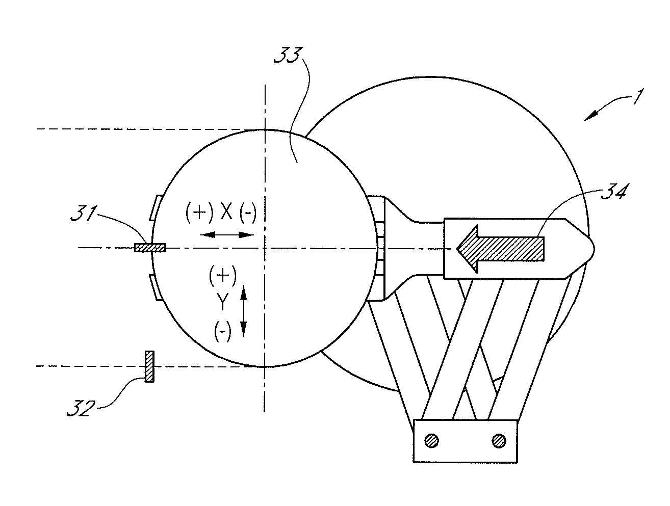
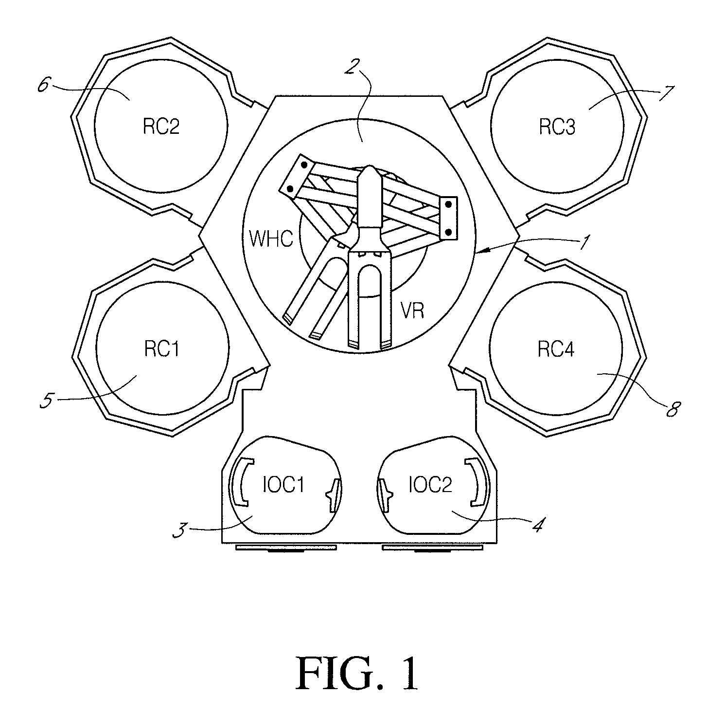
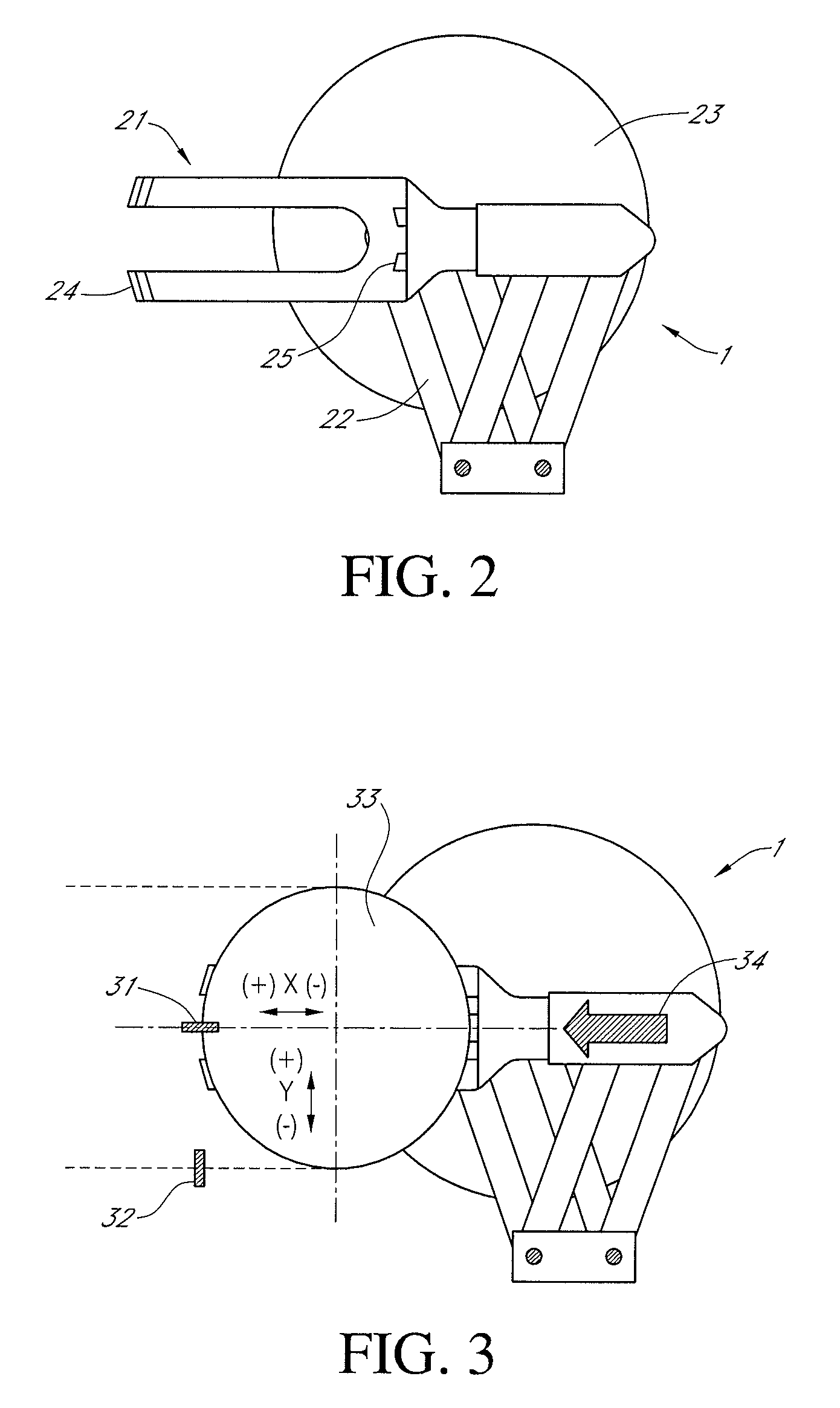
[0029]In an embodiment, a semiconductor-processing apparatus comprises: (I) a wafer handling chamber; (II) at least one wafer processing chamber, each connected to the wafer handling chamber; (III) a wafer handling device disposed in the wafer handling chamber for loading a wafer in the wafer processing chamber, said wafer handling device comprising an end effector for placing a wafer thereon, said end effector being movable from a ready-to-load position to the wafer processing chamber in an x-axis direction which is a wafer loading direction and in a y-axis which is perpendicular to the x-axis direction on a wafer loading plane; (IV) at least one first photosensor disposed in the wafer handling chamber in front of the wafer processing chamber at a position where the wafer placed on the end effector...


PUM


Abstract

A semiconductor-processing apparatus includes: a wafer handling chamber; a wafer processing chamber; a wafer handling device; a first photosensor disposed in the wafer handling chamber in front of the wafer processing chamber at a position where the wafer partially blocks light received by the first photosensor at a ready-to-load position and substantially entirely blocks light received by the first photosensor when the wafer moves from the ready-to-load position toward the wafer processing chamber in the x-axis direction; and a second photosensor disposed in the wafer handling chamber in front of the wafer processing chamber at a position where the wafer does not block light received by the second photosensor at the ready-to-load position and partially blocks light received by the second photosensor when the wafer moves from the ready-to-load position toward the wafer processing chamber in the x-axis direction.

Description

BACKGROUND OF THE INVENTION[0001]1. Field of the Invention[0002]The present invention generally relates to a wafer-processing apparatus provided with a wafer alignment device, and particularly to a wafer handling device compensating for a deviation of a wafer thereon.[0003]2. Description of the Related Art[0004]In recent years, the number of wafers processed per unit time (=throughput) has become a matter of keen interest in connection with semiconductor manufacturing apparatuses used in the production of semiconductors. To improve the throughput, various ideas have been experimented on semiconductor manufacturing apparatuses, such as increasing the number of wafer processing chambers, providing multiple arms on the wafer handling device, and raising the wafer loading speed of the wafer handling device.[0005]However, one major problem remains unaddressed, which is the deviation of wafers on the wafer handling device caused by higher wafer loading speeds. To be specific, when a wafer...

Claims


Application Information

Patent Timeline
Patent Type & Authority Patents(United States)
IPC IPC(8): H01L21/677
CPCH01L21/681H01L21/68707Y10S414/135Y10S414/136G05B19/402G05B2219/37608G05B2219/40562H01L21/67265H01L21/67742
Inventor TAKIZAWA, MASAHIROSUWADA, MASAEIAKAGAWA, MASAYUKI
Owner ASM JAPAN
Why Eureka
Try Eureka