

Surface preparation prior to deposition on germanium
- Summary
- Abstract
- Description
- Claims
- Application Information
AI Technical Summary
Benefits of technology
Problems solved by technology
Method used
Image

Examples
Embodiment Construction
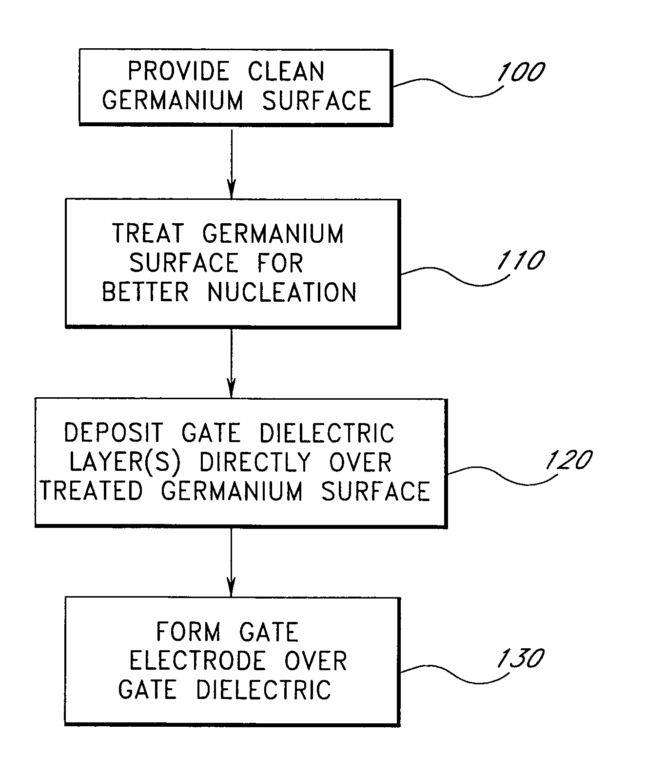
[0022] Treatments are described herein for preparing germanium surfaces for subsequent deposition. The thermal reaction or plasma products preferably modify termination of the germanium surface to make it more uniformly susceptible to subsequent deposition. The treatments preferably provide a consistent density of nucleation sites across the surface. While the treatment processes are described herein in conjunction with adsorption-driven reactions of atomic layer deposition over the treated germanium surface, the skilled artisan will readily appreciate that the methods taught herein will also be applicable to nucleation of other deposition processes for a variety of materials over germanium surfaces.
[0023] Atomic layer deposition (ALD) is a self-limiting process, whereby alternated pulses of reaction precursors saturate a substrate and leave no more than one monolayer of material per pulse. The precursors are selected to ensure self-saturating reactions, because an adsorbed layer i...
PUM
| Property | Measurement | Unit |
|---|---|---|
| Temperature | aaaaa | aaaaa |
| Temperature | aaaaa | aaaaa |
| Percent by atom | aaaaa | aaaaa |
Abstract
Description
Claims
Application Information