Method for fabricating locally strained channel

a fabrication method and local strain technology, applied in the direction of semiconductor devices, electrical equipment, transistors, etc., can solve the problems of short channel effect, junction leakage, new problems, etc., and achieve the effect of increasing the operating speed of the device, increasing the horizontal mobility of electrons in the channel, and increasing the conductivity

Inactive Publication Date: 2005-02-22
MACRONIX INT CO LTD
View PDF2 Cites 65 Cited by
  • Summary
  • Abstract
  • Description
  • Claims
  • Application Information

AI Technical Summary

Benefits of technology

By growing a silicon layer on a SiGe layer, the channel at the strained silicon layer is under biaxial tensile strain. Further with the cap-annealing process, a compressive stress is generated on the n-type gate structure, which in turns introduces tensile strain to the strained silicon layer. The tensile strain of the strained silicon layer enhances the horizontal mobility of electrons in the channel. As a result, the operating speed of a device can also be increased.
For the manufacturing method of a semiconductor device of the present invention, because the source / drain region is located either in the strained silicon layer or in both the strained silicon layer and the SiGe layer with higher conductivity, the resistance of the source / drain region is effectively reduced.
Further, since the resistance of the source / drain region is effectively reduced, the source / drain region can be formed as shallow junctions, thus avoiding short channel effect and junction leakage.
For the semiconductor device of the present invention and the manufacturing method thereof, both the performance and the reliability of the device are improved.

Problems solved by technology

However, if the junction depth of the source / drain region is increased to improve the aforementioned problems, new issues, including short channel effects and junction leakage, can arise.
On the other hand, if heavy dosage implantation is used to reduce the resistance, solid solubility limitation may hamper application of heavy dosage implantation for forming shallow junction for the source / drain regions.
However, the resulted silicided shallow junction may lead to unacceptable junction leakage and further increase the junction resistance.

Method used


Image

  • Method for fabricating locally strained channel
  • Method for fabricating locally strained channel
  • Method for fabricating locally strained channel

Examples


Embodiment Construction

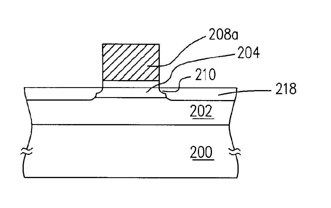
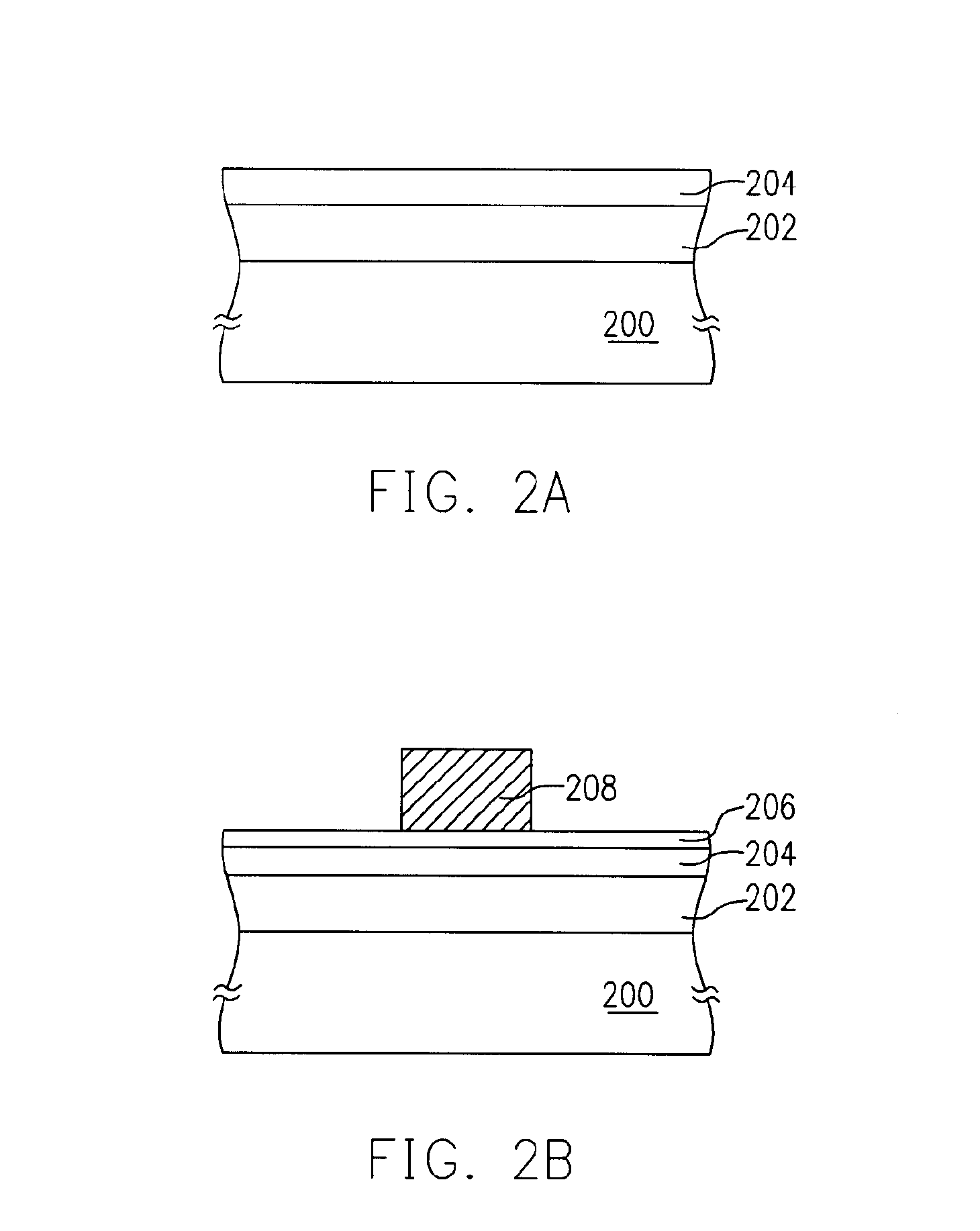
FIGS. 2A-2G are schematic, cross-sectional diagrams to illustrate the process flow for the manufacturing of a semiconductor device according to one aspect of this invention.

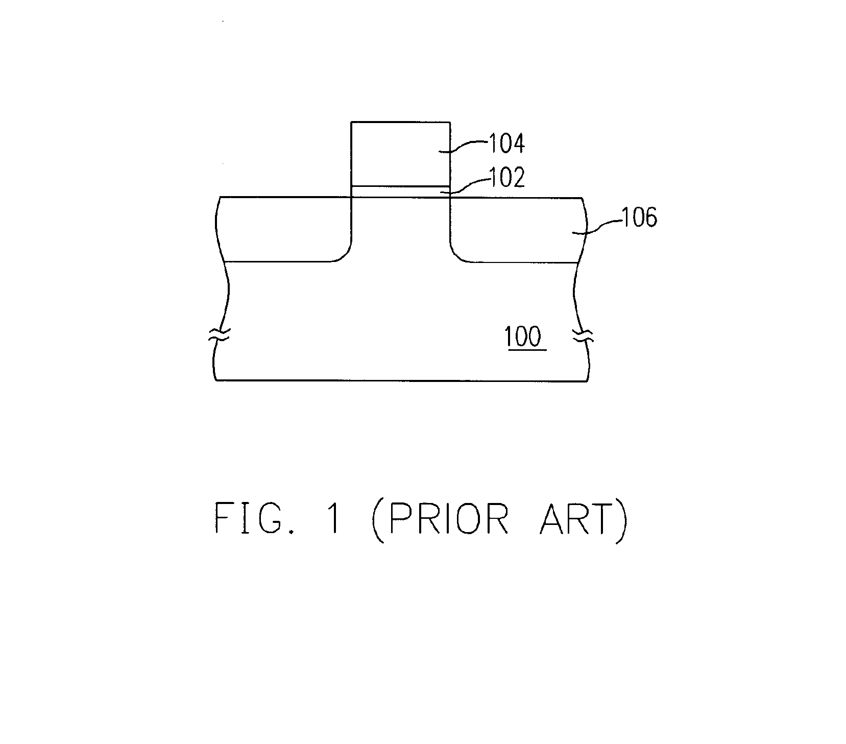
Referring to FIG. 2A, a substrate 200 is provided and a silicon germanium (Si1-xGex; SiGe) layer 202 is formed on the surface of the substrate 200. A strained silicon layer 204 is formed on the SiGe layer 202. The strained silicon layer 204 has a thickness of, for example, about 200 to 1000 angstroms. For example, the SiGe layer 202 and the strained silicon layer 204 are formed by ultra high vacuum chemical vapor deposition (UHV-CVD) on the substrate. The SiGe layer 202 is epitaxially grown on the substrate and the strained silicon layer 204 is epitaxially grown on the SiGe layer 202. For the UHV-CVD process, a reaction gas including Si2H6 / GeH4 is used, with a base pressure of about 2×10⁻¹⁰ Torr, a deposition pressure of less than 1 mTorr and a rising temperature gradient of 150° C. / minute, for example.

Due to the...


PUM


Abstract

A manufacturing method for a semiconductor device is provided, wherein a silicon germanium (Si1-xGex; SiGe) layer and a strained silicon layer are sequentially formed on a semiconductor substrate. A gate oxide layer and a gate structure are further formed on the strained silicon layer. The gate structure and the strained silicon layer are heavily doped with n-type dopants to form a compressed gate and source/drain regions, respectively. A cap layer is further formed over the semiconductor substrate, followed by conducting an annealing process. The cap layer is subsequently removed.

Description

BACKGROUND OF INVENTION1. Field of InventionThe present invention relates to a manufacture method for a semiconductor device. More particularly, the present invention relates to a fabrication method for a semiconductor device with a locally strained channel.2. Description of Related ArtThe metal-oxide-semiconductor (MOS) transistor is an important device applied in very-large-integrated-circuits such as microprocessors and semiconductor memories. In addition to a gate oxide layer and a conductive gate structure, the MOSFET transistor further includes a source / drain region having a conductivity type opposite to that of the substrate.FIG. 1 illustrates the cross-sectional view of a prior-art semiconductor device structure. As shown in FIG. 1, the prior art structure comprises a substrate 100, a gate oxide layer 102, a gate structure 104 and a source / drain region 106. The gate oxide layer 102 is disposed on the surface of a portion of the substrate 100, while the gate structure 104 is ...

Claims


Application Information

Patent Timeline
Patent Type & Authority Patents(United States)
IPC IPC(8): H01L21/02H01L29/10H01L21/336H01L29/02
CPCH01L29/1054H01L29/6659H01L29/665
Inventor CHANG, KENT KUOHUA
Owner MACRONIX INT CO LTD
Why Eureka
Try Eureka