Electronic components

a technology of electronic components and components, applied in the field of low-cost electronic components and circuits, can solve the problems of large capital investment, high cost of final products, and use of dangerous chemicals, and achieve the effects of improving heat transfer, simple process, and accurate placement of nanoparticles

Inactive Publication Date: 2006-10-26
HEWLETT PACKARD DEV CO LP
View PDF13 Cites 78 Cited by
  • Summary
  • Abstract
  • Description
  • Claims
  • Application Information

AI Technical Summary

Benefits of technology

[0007] Furthermore, the use of group IV elements, such as silicon or germanium, when recrystallised provides high electrical performance, which may be significantly higher that that available from organic semiconductors, inorganic oxide semiconductors and compound inorganic semiconducting materials.
[0034] In preferred embodiments of the invention, inkjet printing techniques are used to precisely deliver of fluids carrying nanoparticles of inorganic semiconductor materials and dopants, insulator, conductor, or electrode material etc. on to the surface of the substrate to build up electronic components and circuits. In other embodiments, other printing techniques such as offset lithographic (photogravure) or digital offset printing methods are employed. Using such techniques allows the use of specific high performance materials with which relatively high performance electronic circuits may be produced; thus, providing performance that is significantly higher that than of circuits using semi-conducting polymers, for example. For example, high electron mobility doped silicon or germanium, for use in transistor gates may be employed, together with high conductivity gold and copper contacts. Preferably this is carried out in a completely, or substantially completely, additive process, without the use of expensive or dangerous chemicals. Thus, lower materials costs are incurred and little waste is produced. Consequently, methods according to the invention may have a reduced environmental impact compared to conventional methods.

Problems solved by technology

Additionally, they require the use of dangerous chemicals that necessitate the adoption of stringent safety procedures.
These processes result in the requirement of a large capital investment.
Consequently, the final product is relatively expensive.

Method used


Image

  • Electronic components
  • Electronic components
  • Electronic components

Examples


Embodiment Construction

[0046] There will now be described examples of the best mode contemplated by the inventors for carrying out the invention.

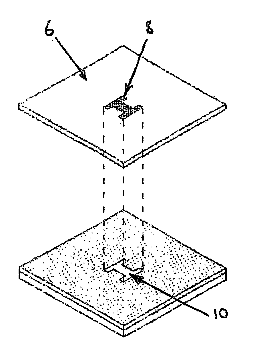
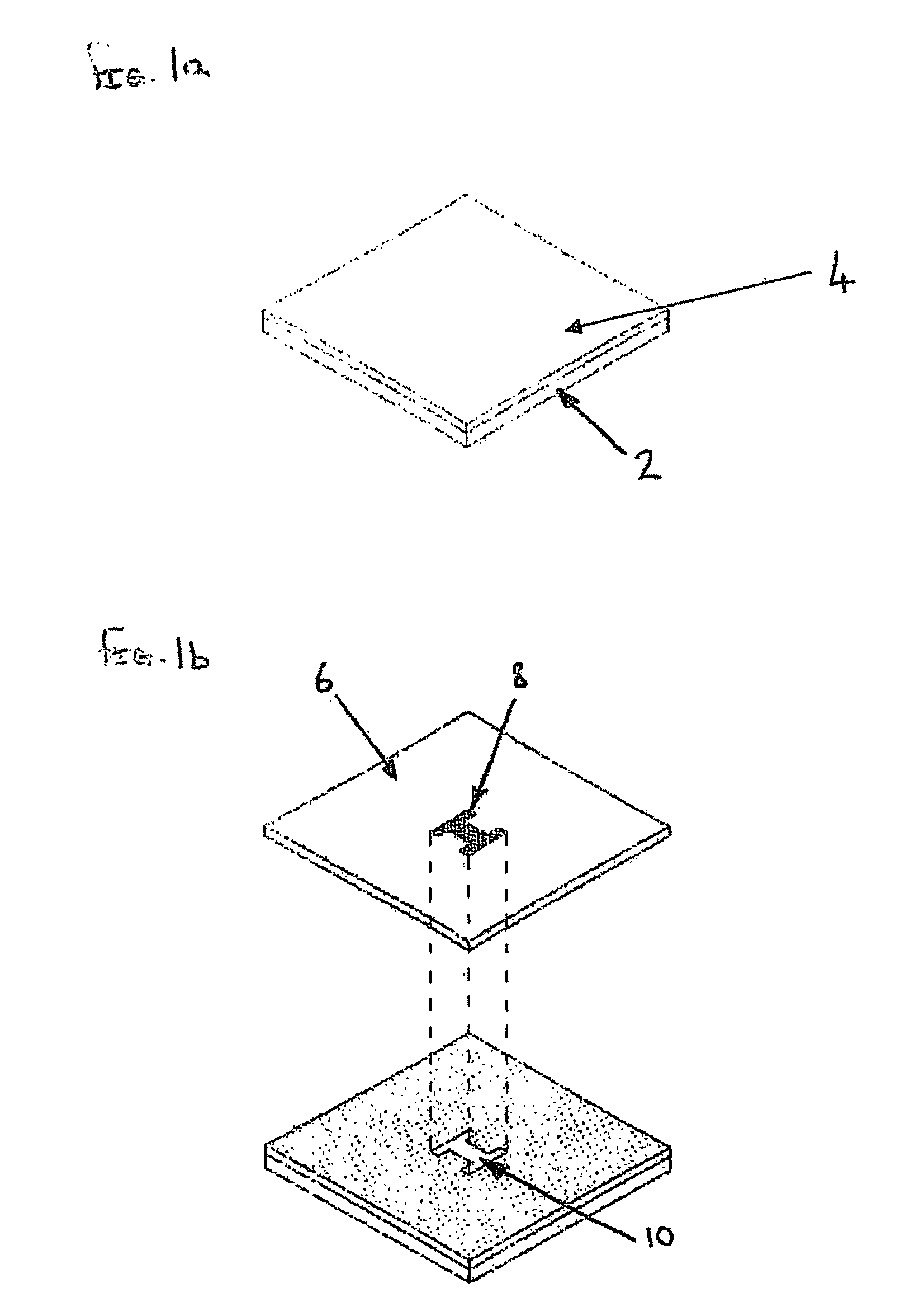
[0047] As has been described above, in preferred embodiments of the invention stamps are inked such that they retain a hydrophobic, liquid on features of their surfaces. The hydrophobic liquid is then transferred through a soft-contact-lithography stamping, or printing process to the desired location on a substrate on which one or more electronic components or circuits are to be constructed. When this same area has hydrophilic solutions or inks deposited on it or adjacent to it, separation occurs between the hydrophobic and hydrophilic regions. This technique is used in preferred embodiments to help define specific or critical dimensions of electrical components such as the dimensions of gates for transistors.

[0048] Below, the manufacturing process for a stamp for use in the present embodiment is described, as are suitable techniques for inking and aligning the...


PUM

PropertyMeasurementUnit
diameteraaaaaaaaaa
depthaaaaaaaaaa
sizeaaaaaaaaaa

Abstract

A method of manufacturing an electronic component comprising at least one n- or p-doped portion, comprising the steps of: co-depositing inorganic semi-conducting nanoparticles and dopant on a substrate, the nanoparticles being a group four element such as silicon or germanium; fusing the nanoparticles by heating to form a continuous layer; and subsequently; and, recrystallising the layer.

Description

FIELD OF THE INVENTION [0001] The present invention relates generally to low cost electronic components and circuitry and to methods and apparatus for manufacturing such electronic components and circuitry. BACKGROUND TO THE INVENTION [0002] Semiconductor fabrication traditionally employs a series of technologically demanding steps. For instance in the case of the manufacture of high performance transistors these may include: vacuum deposition methods to deposit conductors, followed by the application of photo-resist, exposing, developing, etching and then dopant implantation. Such methods must be performed in a clean room environment to prevent contamination of the substrate that would result in gaps in the metal layers or photo-resists. Additionally, they require the use of dangerous chemicals that necessitate the adoption of stringent safety procedures. These processes result in the requirement of a large capital investment. Consequently, the final product is relatively expensive...

Claims


Application Information

Patent Timeline
Patent Type & Authority Applications(United States)
IPC IPC(8): H01L29/04C23C26/02C23C30/00H01L21/20H01L21/208H01L21/268H01L21/336H01L29/786H01L51/40
CPCC23C26/02C23C30/00H01L21/268H01L29/66742H01L29/66765H01L29/78678H01L21/02686H01L51/0004H01L21/02532H01L21/02576H01L21/02579H01L21/02601H01L21/02628H01L29/78684H10K71/13
Inventor COLFER, PAULBYRNE, LORRAINECAHILL, EUGENEKEENAN, PHILSTOBIE, NIALL
Owner HEWLETT PACKARD DEV CO LP
Why Eureka
Try Eureka