
Electronics module having high density interconnect structures incorporating an improved dielectric lamination adhesive

Inactive Publication Date: 2001-09-25
LOCKHEED MARTIN CORP
View PDF4 Cites 136 Cited by
  • Summary
  • Abstract
  • Description
  • Claims
  • Application Information

AI Technical Summary

Benefits of technology

Accordingly, a primary object of the present invention is to provide a high density interconnect laminate adhesive, having improved electrical performance, while maintaining adequate processing properties.

Problems solved by technology

This repairability feature is a substantial advance over prior connection systems in which reworking the system to replace damaged components was either impossible or involved substantial risk to the good components.
Although BCB has adequate planarization properties, because it is spin or spray coated, there is not complete planarization of the polymer layer that is covering a device or other object.
As such, the interconnection of structures or devices intended to operate at extremely high frequencies presents many challenges not faced in the interconnection of digital systems.
As with any electronic module, there are losses inherent when passing current through a conductor.
In a multi-chip module, these losses come from both the plurality of metal layers, as well as the dielectric layers supporting and separating the metal layers.
As the application frequency increases, the losses associated with the dielectric layers begin to dominate.

Method used


Image

  • Electronics module having high density interconnect structures incorporating an improved dielectric lamination adhesive
  • Electronics module having high density interconnect structures incorporating an improved dielectric lamination adhesive

Examples


example 2

We have demonstrated that the adhesion of "KAPTON.RTM." polyimide films to substrates with BCB as a laminate adhesive is dependent on the lamination time and temperature. For these bond tests, the "KAPTON.RTM." polyimide film was given a standard oxygen RIE treatment and was coated with a thin layer of adhesion promoter before the BCB polymer was spin coated from a commercially available solution. The structure was then baked for 1 / 2 hour at 100.degree. C., and for 1 / 2 hr at 150.degree. C. to leave a 12 micron thick film. From the results of these tests, shown in Table 2, the minimum time and temperature for good adhesion of the polyimide to other materials was shown to be dependent on temperature and time.

To provide adequate bonding, the temperature should be at least 190.degree. C., and the dwell time at this temperature should be at least 2 hours. However, at higher temperatures, shorter dwell times could be used. For example, a lamination at 230.degree. C. gave good adhesion aft...

example 3

Illustratively, benzocyclobutene can be used as a laminate adhesive by coating BCB on a suitable film material, baking the polymer to B-stage, and then laminating over the desired structure. Specifically, the BCB polymer is supplied as a 57% solution in mesitylene. A 1 mil thick film of "KAPTON E.RTM." polyimide is mounted securely on an 8 inch frame. The frame is cleaned and coated with a silane coupling agent prior to being coated with the adhesive. The frame is placed on a spin coater and the BCB solution dispensed and spun to produce a 12 micron thick adhesive layer (after baking). The baking cycle is 15 minutes at 100.degree. C. followed by 1 hour at 180.degree. C. Laminations are completed using a Carver press modified to deliver pressure and vacuum. "KAPTON.RTM." polyimide sheets are placed on the bottom tray with slits to provide vacuum. The samples are placed face up in the center of the tray, and the frame (with the BCB adhesive) is placed face down onto the sample. The "l...


PUM

PropertyMeasurementUnit
Thicknessaaaaaaaaaa
Thicknessaaaaaaaaaa
Thicknessaaaaaaaaaa

Abstract

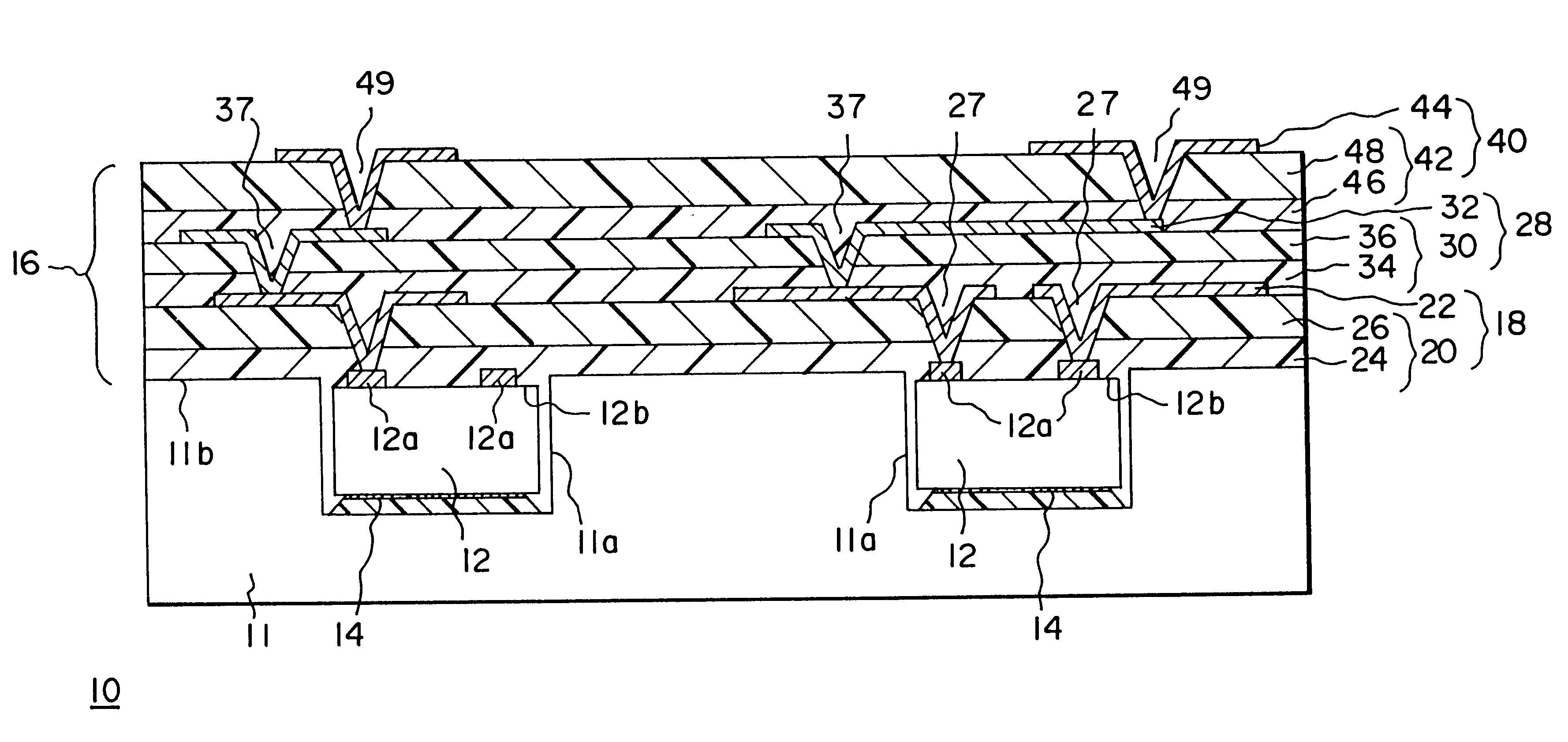
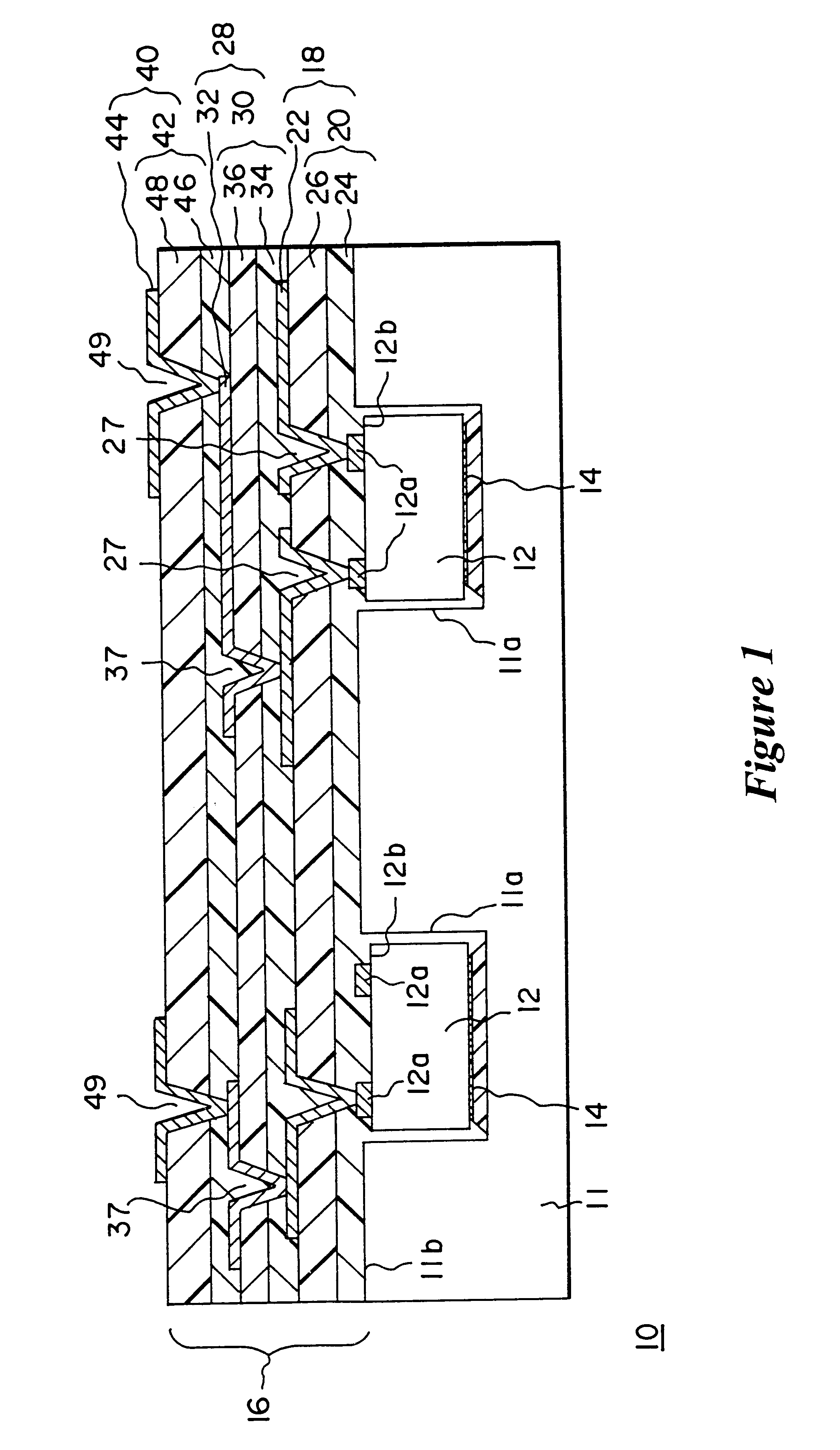
A multi-chip electronics module is provided which utilizes benzocyclobutene as a laminate adhesive for bonding the upper dielectric films in a high density interconnect structure. The benzocyclobutene thermosetting polymer is spin coated on a polyimide film, and baked at low temperature to remove any solvent to leave a B-staged coating on the polyimide film. The composite film can be laminated to an underlying electrical structure using a vacuum laminator and heat. As the heat is applied, the BCB layer softens, flows and then cures to bond the polyimide film to the underlying electrical structure.

Description

The present invention relates to an electronics module having an improved dielectric adhesive material and, more particularly, to the use of benzocyclobutene polymer as a laminate adhesive in the construction of the high density interconnect structure of a multi-chip module.A high density interconnect (HDI) structure offers many advantages in the compact assembly of electronic systems. For example, a multi-chip electronic system (such as a microcomputer incorporating 30-50 chips) can be fully assembled and interconnected by a suitable HDI structure on a single substrate, to form a unitary package which is 2 inches long by 2 inches wide by 0.050 inches thick. Even more important, the interconnect structure can be disassembled from the substrate for repair or replacement of a faulty component and then reassembled without significant risk to the good components incorporated within the system. This is particularly important where many (e.g., 50) chips, each being very costly, may be inc...

Claims


Application Information

Patent Timeline
IPC IPC(8): H01L21/02H01L23/52H01L23/28H01L21/58H01L21/70H01L23/29H01L23/538H01L21/98H05K3/46H05K3/38
CPCH01L23/293H01L24/24H01L24/82H01L24/83H01L25/50H05K3/4655H01L23/5389H01L24/19H01L24/29Y10T29/49163H01L2224/2402H01L2224/24227H01L2224/73267H01L2224/8319H01L2224/8388H01L2924/01005H01L2924/01013H01L2924/01018H01L2924/01027H01L2924/01029H01L2924/01074H01L2924/07802H01L2924/14H01L2924/15153H01L2924/15165H01L2924/30105H01L2924/3011H05K3/386H05K3/4652H05K2201/0154H05K2201/0195Y10T29/49165Y10T29/49133Y10T29/49156Y10T29/49146H01L2224/04105Y10S428/901H01L2924/0665H01L2224/2919H01L2224/32225H01L2924/01006H01L2924/01033H01L2924/00H01L2924/12042H01L2924/15787
Inventor COLE, JR., HERBERT STANLEYSITNIK-NIETERS, THERESA ANN
Owner LOCKHEED MARTIN CORP
Learn More