Iron Pyrite Nanocrystal Film As A Copper-Free Back Contact For Polycrystalline CdTe Thin Film Solar Cells

Active Publication Date: 2016-12-01
UNIVERSITY OF TOLEDO
View PDF5 Cites 0 Cited by
  • Summary
  • Abstract
  • Description
  • Claims
  • Application Information

AI Technical Summary

Benefits of technology

[0011]In a fifth aspect of the invention, an FeS2 layer applied as a constituent of the back contact of a photovoltaic cell may provide passivation of pinholes and other shunt-forming defects associated with semiconductor layers. In particular, an embodiment of this aspect of the invention includes a CdS/CdTe semicon

Problems solved by technology

Previous attempts at creating FeS2-based PV devices have performed poorly compared with devices based on other absorber materials (e.g. CdTe, CIGS, CZTS, perovskites such as methylammonium lead iodide, and PbS quantum dots).
This poor efficiency for FeS2-based solar cells is ba

Method used


Image

  • Iron Pyrite Nanocrystal Film As A Copper-Free Back Contact For Polycrystalline CdTe Thin Film Solar Cells
  • Iron Pyrite Nanocrystal Film As A Copper-Free Back Contact For Polycrystalline CdTe Thin Film Solar Cells
  • Iron Pyrite Nanocrystal Film As A Copper-Free Back Contact For Polycrystalline CdTe Thin Film Solar Cells

Examples


Example

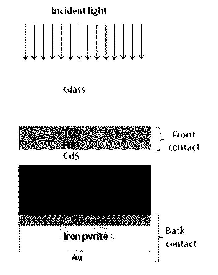
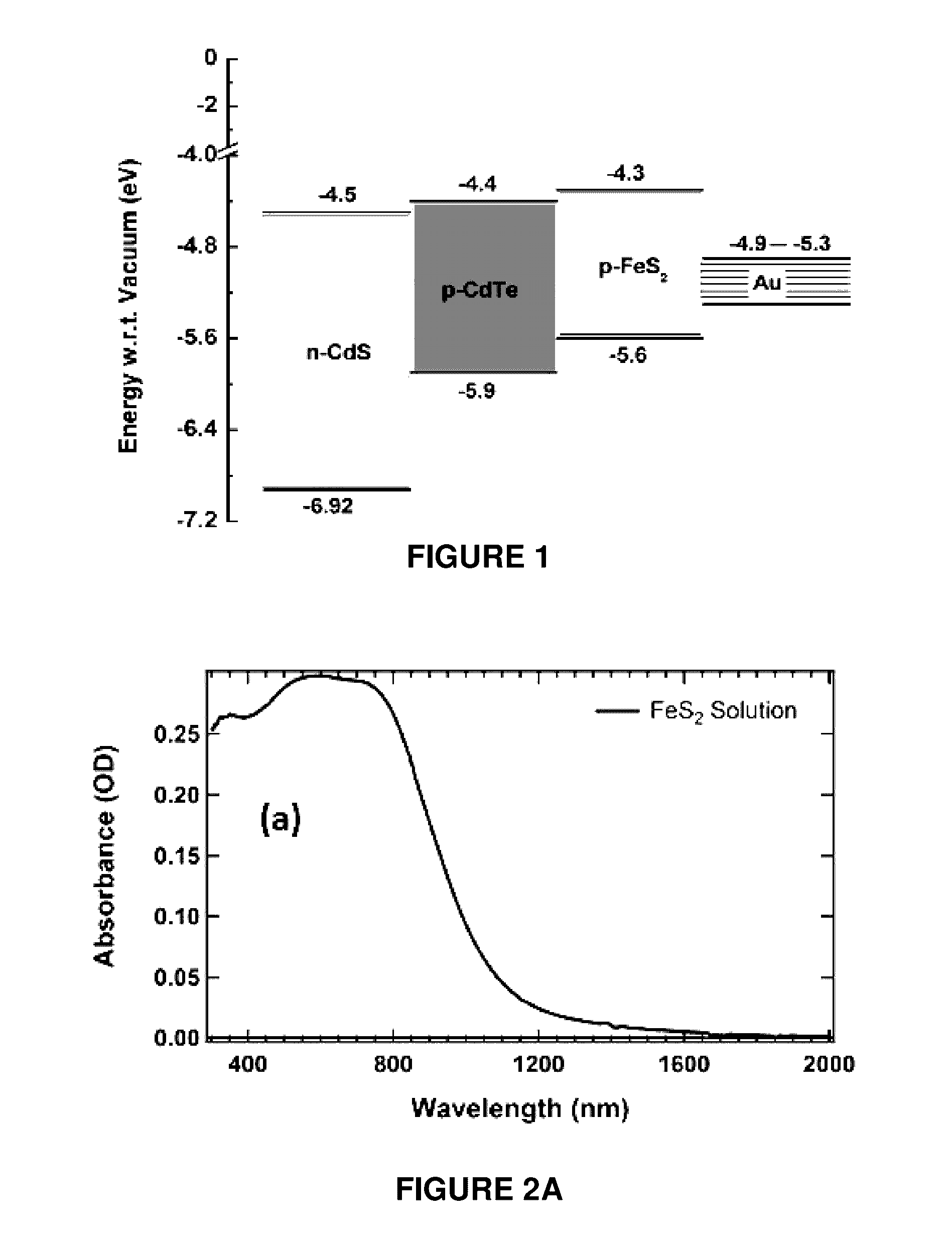
[0046]In a first aspect, there is provided herein an iron pyrite (iron persulfide, FeS2) nanocrystal-based thin film low barrier back contact to CdTe solar cells. While the semiconductor layers are described in the context of CdS and CdTe layers, other materials may be used. For example, the various semiconductor active layers may alternatively be formed from CIGS (copper indium zinc gallium di-selenide), CZTS (copper zinc tin sulfide), CZTSSe (copper zinc tin sulfur selenium alloy), tin sulfide, and copper antimony sulfide. In one embodiment, the FeS2-based back contact can be applied to the cell without pre-treatment of the CdTe p-type film. Creating a low-barrier, ohmic back contact to CdTe often involves addressing both the high work function and the low resistivity of the thin film. Standard back contact preparation often introduces copper, as a thin evaporated layer or as a CuCl2 solution deposition, followed by thermally-assisted diffusion to create a low-resistivity CuxTe ph...


PUM


Abstract

The invention discloses nanocrystalline (NC) FeS2 thin films as the back contact for CdTe solar cells. In one example, the FeS2 NC layer is prepared from a solution directly on the CdTe surface using spin-casting and chemical treatment at ambient temperature and pressure, without a thermal treatment step. Solar cells prepared by applying the NC FeS2 back contact onto CdTe yield efficiencies of about 95% to 100% that of standard Cu/Au back contact devices. In another example, FeS2 is interposed between Cu and Au to form a Cu/FeS2 NC/Au back contact configuration yielding an efficiency improvement of 5 to 9 percent higher than standard Cu/Au devices.

Description

STATEMENT REGARDING SPONSORED RESEARCH[0001]This invention was made with government support under Grant Number CHE-1230246 awarded by the National Science Foundation and also under Grant Number FA9453-11-C-0253 awarded by the Air Force Research Laboratory. The government has certain rights in the invention.FIELD OF THE INVENTION[0002]This invention is generally directed to photovoltaic cells. In particular, this invention relates to FeS2 applied as an ohmic or low barrier back contact material to a photovoltaic cell. In one particular aspect of the invention nanocrystalline (NC) FeS2 thin films are applied as the back contact for CdTe solar cells.BACKGROUND OF THE INVENTION[0003]There is no admission that the background art disclosed in this section legally constitutes prior art.[0004]Photovoltaic cells are devices that convert light energy into electrical energy. Typical photovoltaic cells include a substrate layer for mounting the cell and two ohmic contacts or electrode layers fo...

Claims


Application Information

Patent Timeline
IPC IPC(8): H01L31/0224H01L31/02H01L31/073
CPCH01L31/022441H01L31/02008H01L31/022466H01L31/073H01L31/022425H01L31/0296H01L31/032H01L31/03925Y02E10/543
Inventor BHANDARI, KHAGENDRAELLINGSON, RANDY J.KHANAL, RAJENDRA R.
Owner UNIVERSITY OF TOLEDO
Why Eureka
Try Eureka