Method for avoiding polysilicon defect

Inactive Publication Date: 2008-06-05
SEMICON MFG INT (SHANGHAI) CORP
View PDF23 Cites 1 Cited by
  • Summary
  • Abstract
  • Description
  • Claims
  • Application Information

AI Technical Summary

Benefits of technology

[0029]The embodiments of the invention are advantageous over the prior art in the following. The silicon nitride layer is formed after the polysilicon plug is fabricated, and during the subsequent etching, there will no reaction of the HSC1 with the polysilicon plug due to the protection b

Problems solved by technology

As the integration level of semiconductor devices in integrated circuit fabricating process increases continuously, the density of storage cells of the dynamic random access memory tends to be increasingly large, and thus, the area of a storage cell of the dynamic random access memory available for the capacitor tends to be increasingly small.
When the width of the opening 119 is increased, the silicon nitride layer (as shown with ellipses in the figure) is not removed at the opening 119 because the HSC1 and the BOE can not the etch silicon nitride, which may result in unevenness upon subsequent filling of polysilicon.
Since the HSC1 may react with the polysilicon

Method used


Image

  • Method for avoiding polysilicon defect
  • Method for avoiding polysilicon defect
  • Method for avoiding polysilicon defect

Examples


Example

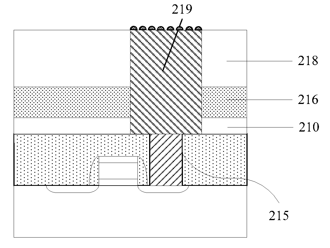
[0035]In the formation of a polysilicon layer during the fabrication of a capacitor in a dynamic random access memory in the prior art, the first interlayer dielectric layer is made of TEOS, and the second interlayer dielectric layer is made of BPSG; the dry etching gas has different etching rates for TEOS and BPSG; consequently, the opening width of the first interlayer dielectric layer and that of the second interlayer dielectric layer are different. Therefore, the HSC1 is required to etch the opening width of the first interlayer dielectric layer and that of the second interlayer dielectric layer to be equal to each other. However, the HSC1 may react with the polysilicon plug, and a defect may occur in the polysilicon plug, resulting in an electric failure. Furthermore, when the HSC1 and the BOE are used to etch the interlayer dielectric layers, there may be a residual of the silicon nitride layer due to the fact that HSC1 and the BOE are unable to etch the silicon nitride layer,...


PUM


Abstract

A method for avoiding a polysilicon defect includes: forming a silicon oxide layer on a silicon substrate; forming a polysilicon plug in the silicon oxide layer, with the polysilicon plug going through the silicon oxide layer; forming on the silicon oxide layer a silicon nitride layer covering the polysilicon plug; forming interlayer dielectric layers on the silicon nitride layer; etching the interlayer dielectric layers over the polysilicon plug to form an opening; etching the silicon nitride layer at the opening to expose the polysilicon plug; and filling polysilicon into the opening such that the opening is in communication with polysilicon plug. In this way, there will be no reaction of the HSC1 with the polysilicon plug due to the protection by the silicon nitride layer. Moreover, since the silicon nitride layer is the last to be etched, there will be no residual thereof, enabling a subsequent flat filling.

Description

CROSS-REFERENCE TO RELATED APPLICATIONS[0001]This application is claiming priority of Chinese Application No. 200610119058.3 filed Dec. 4, 2006, entitled “Method for Avoiding Polysilicon Defect” which application is incorporated by reference herein in its entirety.FIELD OF THE INVENTION [0002]The present invention relates to a method for fabricating a semiconductor memory device, and more particularly to a method for avoiding a polysilicon defect.BACKGROUND OF THE INVENTION [0003]The dynamic random access memory as a widely used integrated circuit device is typically consisted of a transistor and a capacitor. The capacitor is used for storing charges to provide electric information, and hence shall have a sufficiently large capacitance so as to prevent loss of data and to lower the frequency of refreshing.[0004]As the integration level of semiconductor devices in integrated circuit fabricating process increases continuously, the density of storage cells of the dynamic random access ...

Claims


Application Information

Patent Timeline
IPC IPC(8): H01L21/311
CPCH01L21/31111H01L27/10852H01L21/31116H10B12/033
Inventor YANG, YUNYANG, ZHENLIANGKIM, HYUN JAEWANG, GANGNING
Owner SEMICON MFG INT (SHANGHAI) CORP
Why Eureka
Try Eureka