Method for preparing a semiconductor package

Active Publication Date: 2018-09-20
INPAQ TECH
View PDF9 Cites 2 Cited by
  • Summary
  • Abstract
  • Description
  • Claims
  • Application Information

AI Technical Summary

Benefits of technology

[0016]The present disclosure also provides a method for preparing a semiconductor package with a new structure. Regardless whether the desired package size is the standard size 0201, or a larger standard size such as 0402 or DFN10, and even with limited wafer area, the present disclosure still can provide more dies by the method, and sizes of the dies after the singulation process can meet the desired package size. In view of this, the disclosed semiconductor package can be prepared by the method capable of reducing the manufacturing cost. Furthermore, the die is encapsulated without high dielectric constant materials, but instead using protecting materials of the dry film process. Accordingly, the parasitic effect is relatively insignificant. In addition, the present disclosure uses conductive elements instead of conductive wirings to electrically connect the die and the carrier substrate, so that the parasitic effect is not likely to occur. For this reason, when the die operates at a high frequency, the influence of the parasitic effect on the die is relatively small, so the electrical performance is improved.
[0017]In contrast, in conventional semiconductor packages, the size of the die is equal to that of the semiconductor package. For instance, if the size of the semiconductor package is the standard size 0201, the size of the die is the standard size 0201 as well. Accordingly, with wafer sections of comparable size, a greater number of dies can b

Problems solved by technology

However, the dielectric constant of the molding is relatively high, which causes relatively high parasitic effect (e.g., parasitic capacitance or parasitic resistance) in the conventional semiconductor packages.
The length of the metal wirings is relatively longer in the conventional semiconductor packages as compared to the metal wirings of the disclosed semiconductor package, resulting in increased parasitic effect under the conventional semiconductor packages.
Therefore, when the die operates at high frequency, t

Method used


Image

  • Method for preparing a semiconductor package
  • Method for preparing a semiconductor package
  • Method for preparing a semiconductor package

Examples


Example

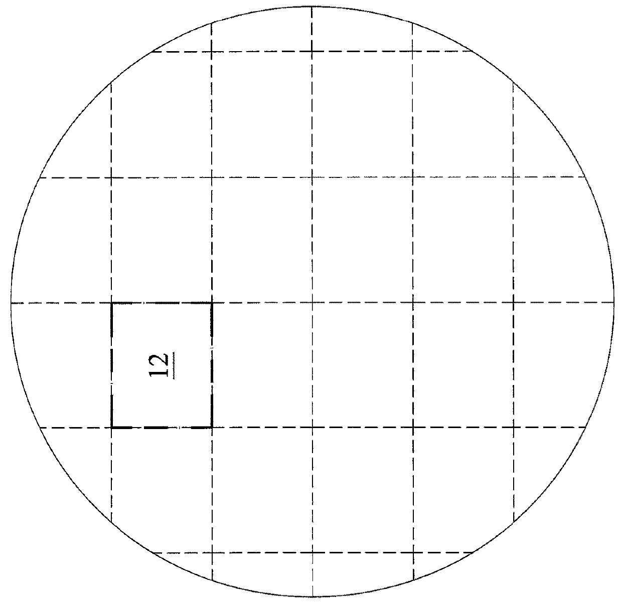
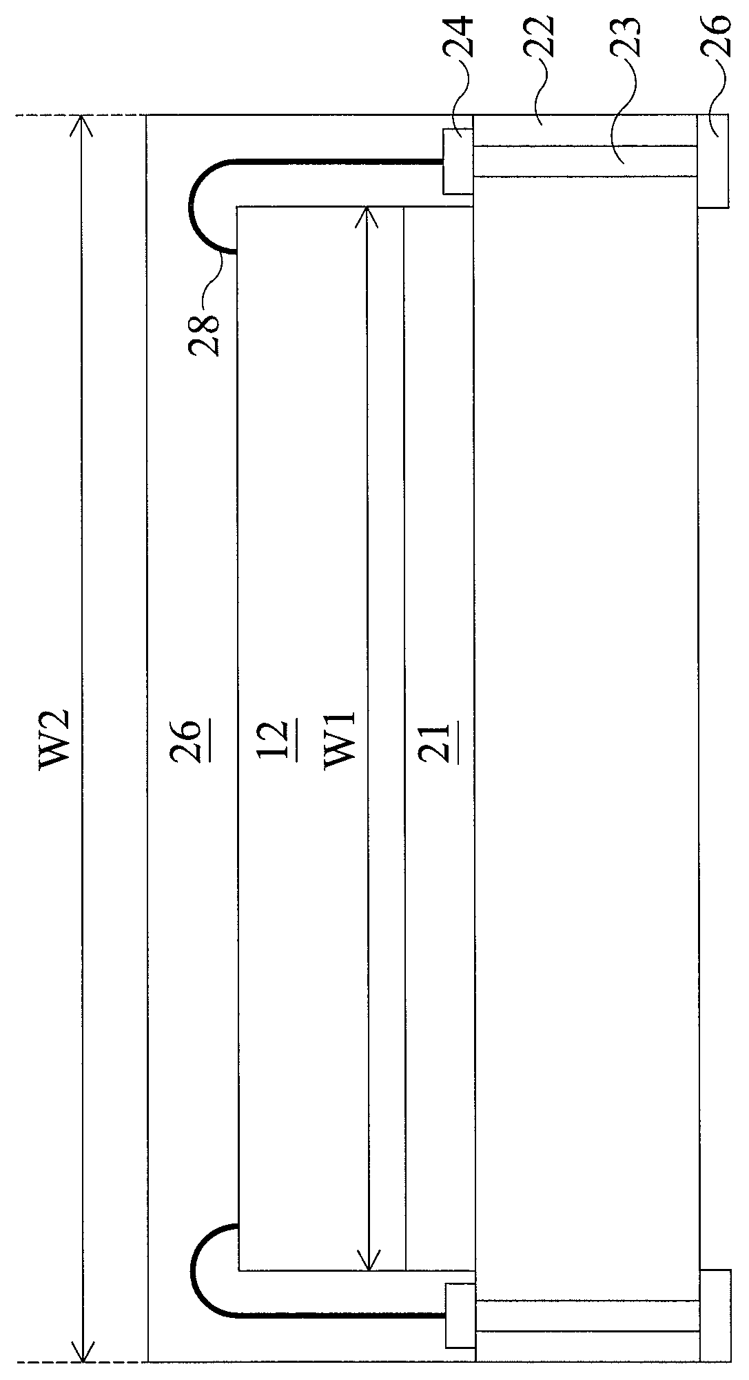
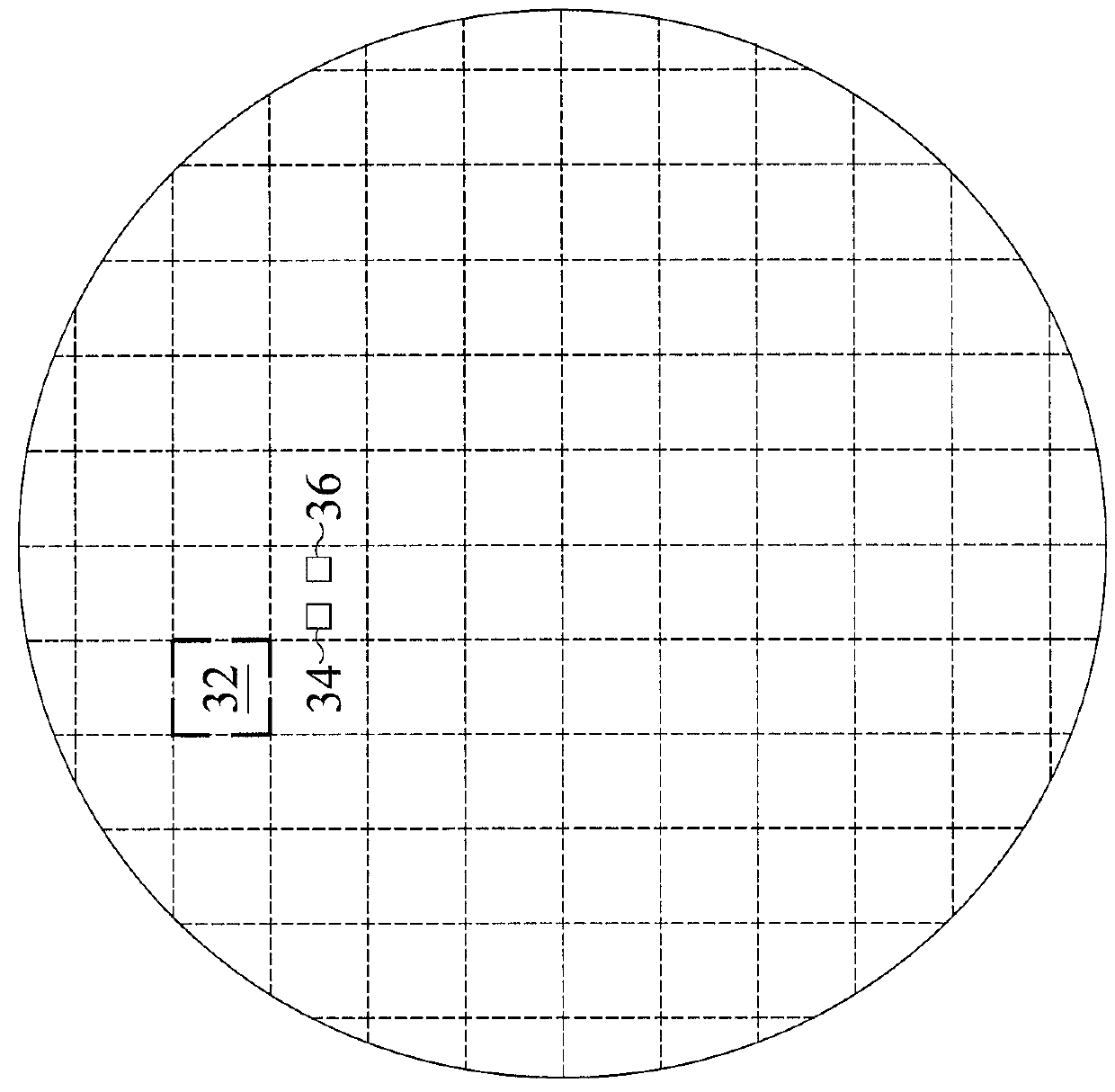
[0024]The present disclosed embodiments and examples as shown in the figures are illustrated by using particular language. It should be understood that no limitation of the scope of the present disclosure is thereby intended. Any alterations and any modifications disclosed in the embodiment, as well as any further applications of the principles disclosed in the description, shall be deemed to be common knowledge for those skilled in the art. The reference numerals may be repeated throughout the embodiments, but this does not necessarily require that the features of one embodiment apply to another embodiment, even if they share the same reference numeral. It will be understood that when an element is referred to as being “connected to” or “coupled with” another element, it may be regarded as being directly connected or being coupled to another element, or intervening elements may exist therebetween.

[0025]Moreover, spatial relation terms, such as “below,”“under,”“beneath,”“above,”“ove...


PUM


Abstract

The present disclosure provides a method for preparing a semiconductor package having a standard size from a die having a size smaller than the standard size. The method includes: providing a wafer; forming a die on the wafer, wherein the die has a size smaller than one-half of a standard size 0201; dicing the die from the wafer; encapsulating the die to form an encapsulated die; and singulating the encapsulated die to form a semiconductor package having a size equal to or larger than the standard size 0201.

Description

CROSS-REFERENCE TO RELATED APPLICATION[0001]The present application is based on, and claims priority from, Taiwan Patent Application Serial Number 106108726, filed on Mar. 16, 2017, the disclosure of which is hereby incorporated by reference herein in its entirety.TECHNICAL FIELD[0002]The present disclosure generally relate to a method for preparing a semiconductor package, and more particularly, to a method for preparing a semiconductor package having a standard size from a die having a size smaller than the standard size.DISCUSSION OF THE BACKGROUND[0003]Within the electronics industry, vigorous development has focused on multi-functional and high-performance capabilities of electronic products. To meet the integration and miniaturization packaging requirements of semiconductor package structures, circuit board designs for carrying active and passive components and wirings have evolved from single-layer to multi-layer board designs. With a multi-layer board, an area of wire routin...

Claims


Application Information

Patent Timeline
IPC IPC(8): H01L23/00H01L21/56H01L21/78H01L23/498H01L23/29H01L21/48H01L23/31
CPCH01L24/97H01L21/561H01L21/78H01L23/3121H01L23/293H01L21/4867H01L23/49838H01L23/49816H01L23/49827H01L2224/48091H01L2224/48227H01L2224/73265H01L2224/32225H01L2224/48235H01L24/48H01L24/32H01L24/16H01L2224/16235H01L2224/13294H01L2224/13311H01L2224/13339H01L2224/13193H01L2224/13386H01L2224/1132H01L2224/113H01L2224/1144H01L2224/1131H01L24/11H01L2924/181H01L2224/97H01L24/81H01L2224/92247H01L24/13H01L24/83H01L24/85H01L2224/131H01L2924/00014H01L2924/01006H01L2924/014H01L2224/81H01L2224/45099H01L2924/00H01L2224/16225
Inventor PENG, YU-MINGHSU, CHU-CHUNKO, HUNG-SHUNGYEH, HSIU-LUN
Owner INPAQ TECH
Why Eureka
Try Eureka