Integrated circuit package and method for fabricating same

a technology of integrated circuits and plastic packages, which is applied in the direction of semiconductor devices, semiconductor/solid-state device details, electrical equipment, etc., can solve the problems of reducing size and manufacturing costs, and achieve the effects of improving electrical performance, good thermal path for thermal dissipation, and reducing electrical impedance of gold wires

Active Publication Date: 2008-03-25
UTAC HEADQUARTERS PTE LTD
View PDF56 Cites 136 Cited by
  • Summary
  • Abstract
  • Description
  • Claims
  • Application Information

AI Technical Summary

Benefits of technology

[0007]Advantageously, integrated circuit package according to embodiments of the present invention includes an air cavity through which the wire bonds travel. Thus, the wires between the semiconductor die and the contact pads span an air gap rather than traveling through mold compound. The air has a lower dielectric constant than mold compound and therefore the electrical impedance of the gold wire is much lower when the wire runs through air rather than through mold compound. Thus signal distortion at high frequencies is inhibited. Additionally, semiconductor dice that are sensitive to pressure, including MEMS (micro electro-mechanical systems), GaAs dice etc. are less likely to be damaged during assembly as there is no molding material molded in a pressurized molding step.
[0008]Also, the die attach pad provides a good thermal path for thermal dissipation from the semiconductor die. The contact pads allow for different design variations since there is no lead connection as in the leadless plastic chip carrier. In the embodiment including the moat around each contact pad, signals are shielded by grounding for increased electrical performance.

Problems solved by technology

However, further developments in IC packaging are driven by specific applications and continued demand for improved reliability, electrical performance, decreased size and cost of manufacture.

Method used


Image

  • Integrated circuit package and method for fabricating same
  • Integrated circuit package and method for fabricating same
  • Integrated circuit package and method for fabricating same

Examples


Embodiment Construction

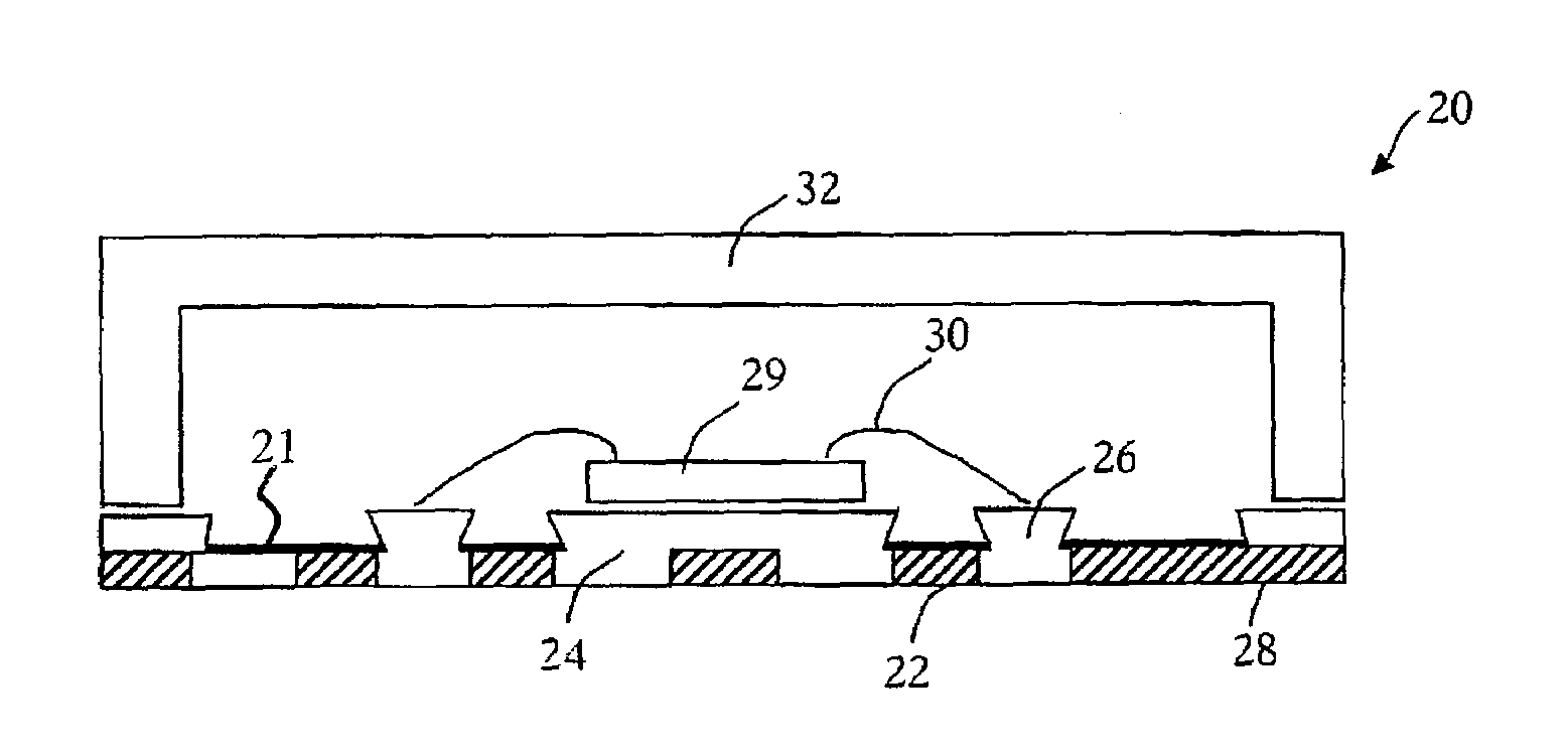
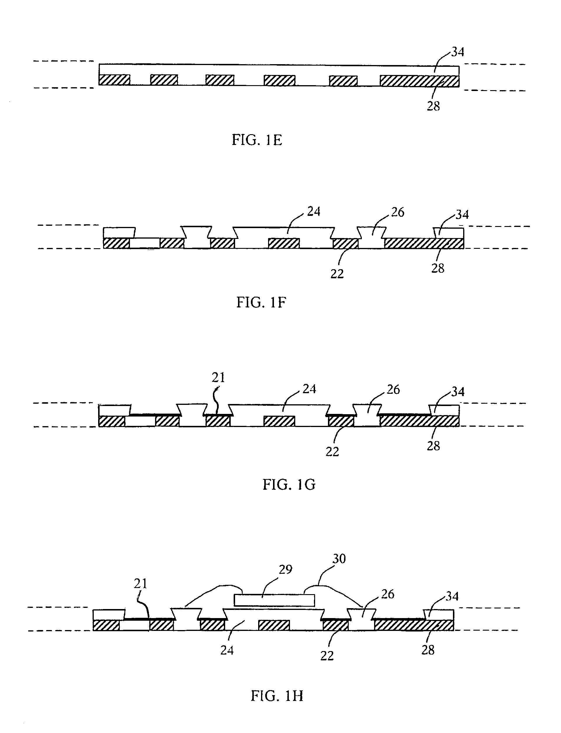
[0016]Reference is made to FIGS. 1A to 1J to describe a process for manufacturing an integrated circuit package according to one embodiment of the present invention and indicated generally by the numeral 20. The integrated circuit package 20 is best shown in FIG. 1J and includes a package base 22 that includes a die attach pad 24 and a plurality of contact pads 26 in a non-conductive material 28. A semiconductor die 29 is mounted to the die attach pad 24 and wire bonds 30 connect the semiconductor die 29 to various ones of the contact pads 26. A lid 32 is fixed to the package base 22 and covers the semiconductor die 29 and the wire bonds 30.

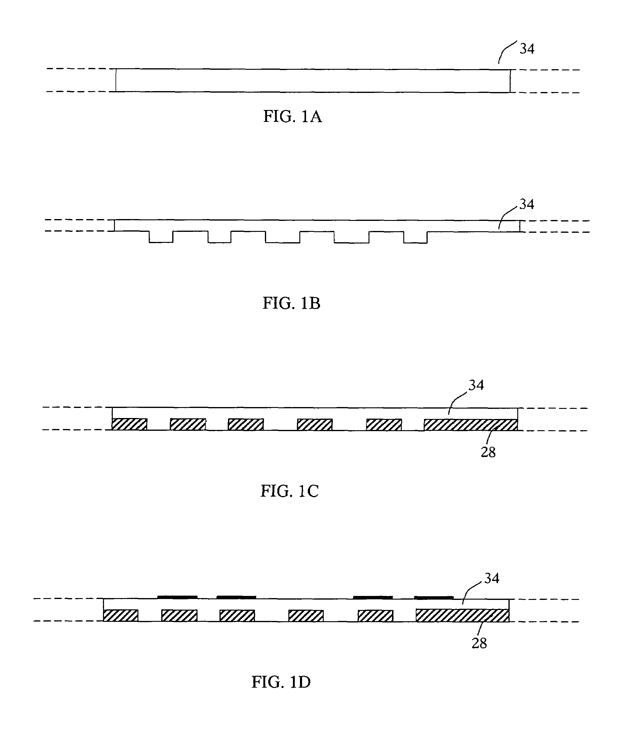
[0017]A process for manufacturing the integrated circuit package 20 will now be described in more detail, with continued reference to FIGS. 1A to 1J. FIG. 1A shows a sectional side view of a Cu (copper) panel substrate 34 which forms the raw material of a leadframe strip. As discussed in detail in Applicant's own U.S. Pat. No. 6,229,200, the lead...


PUM


Abstract

A process for fabricating an integrated circuit package includes: selectively etching a first side of a substrate thereby providing etched regions of the substrate to partially define at least a plurality of contact pads; adding a dielectric material to the etched regions of the substrate; selectively etching a second side of the substrate to further define at least the plurality of contact pads and thereby provide a package base of at least the contact pads and the dielectric; mounting a semiconductor die to the package base and connecting the semiconductor die to the contact pads; fixing a lid to the package base to cover the semiconductor die in a cavity between the lid and the package base; and singulating to provide the integrated circuit package.

Description

FIELD OF THE INVENTION[0001]The present invention relates generally to integrated circuit packaging and more particularly to a thin array plastic package and a process for fabricating the thin array plastic package.BACKGROUND OF THE INVENTION[0002]An etch back process for fabricating an integrated circuit package is disclosed in U.S. Pat. No. 6,498,099, assigned to the assignee of the present application, the entire contents of which are incorporated herein by reference. According to this process, a copper substrate strip is first subjected to a partial etch on one or both of the top and bottom surfaces to create a pattern of contact leads (pads) and a die attach pad (paddle). After wire bonding the contacts to a singulated semiconductor die, followed by overmolding and curing of the mold, the leadframe strip is exposed to a second immersion etch for exposing the contact pads in an array pattern (i.e. multi-row) or perimeter pattern (i.e. single row), as well as the die attach pad. ...

Claims


Application Information

Patent Timeline
Patent Type & Authority Patents(United States)
IPC IPC(8): H01L23/12H01L23/10
CPCH01L21/4828H01L23/055H01L24/32H01L23/10H01L23/49548H01L24/48H01L2924/1461H01L2924/0132H01L2924/01033H01L2224/16245H01L2924/3025H01L2924/3011H01L2924/16152H01L2924/14H01L2924/10329H01L2924/09701H01L2924/014H01L2924/01082H01L2924/01079H01L2924/01078H01L2924/01047H01L2924/01046H01L2924/01029H01L2924/01028H01L24/45H01L2224/32014H01L2224/32245H01L2224/45144H01L2224/48091H01L2224/48247H01L2224/484H01L2224/48599H01L2224/73265H01L2224/92247H01L2924/01015H01L2924/01027H01L2924/00014H01L2924/00012H01L2924/01031H01L2924/00H01L2924/15747H01L2924/181H01L24/73H01L2224/85399H01L2224/05599
Inventor KIRLOSKAR, MOHANWAGENHOFFER, KATHERINEHIGGINS, III, LEO M.
Owner UTAC HEADQUARTERS PTE LTD
Why Eureka
Try Eureka