Voltage droop suppressing active interposer

Inactive Publication Date: 2005-12-29
NAIR RAJENDRAN
View PDF6 Cites 12 Cited by
  • Summary
  • Abstract
  • Description
  • Claims
  • Application Information

AI Technical Summary

Benefits of technology

[0009] The invention proposes an interposer assembly architecture for noise suppression circuits on a CPU package. In this architecture, called the “Transient Suppressing Active Interposer”, charge is stored on dedicated capacitors at a voltage substantially higher than the operating voltage of the CPU. These capacitors are mounted upon the active circuits that are packaged to match the size and form factor of the capacitors and this assembly is then attached to the package substrate. Charge is conveyed to the capacitors dedicated to the active noise suppression function through electrical circuit pathways in the package substrate. These circuit pathways connect to the capacitor terminals through the package of the active noise suppression devices. Depending upon the capacitor construction, these terminals may either be double-sided contact terminals along the edge o

Problems solved by technology

Greater levels of integration of transistors devices within a microprocessor, a consequence of device scaling, leads to greater power consumption despite the reduction in operating voltages.
This leads to increasing operating currents, and consequently an increased need for stored charge in close proximity to the microprocessor.
The active devices occupy real-estate on the package substrate, displacing capacit

Method used


Image

  • Voltage droop suppressing active interposer
  • Voltage droop suppressing active interposer
  • Voltage droop suppressing active interposer

Examples


Example

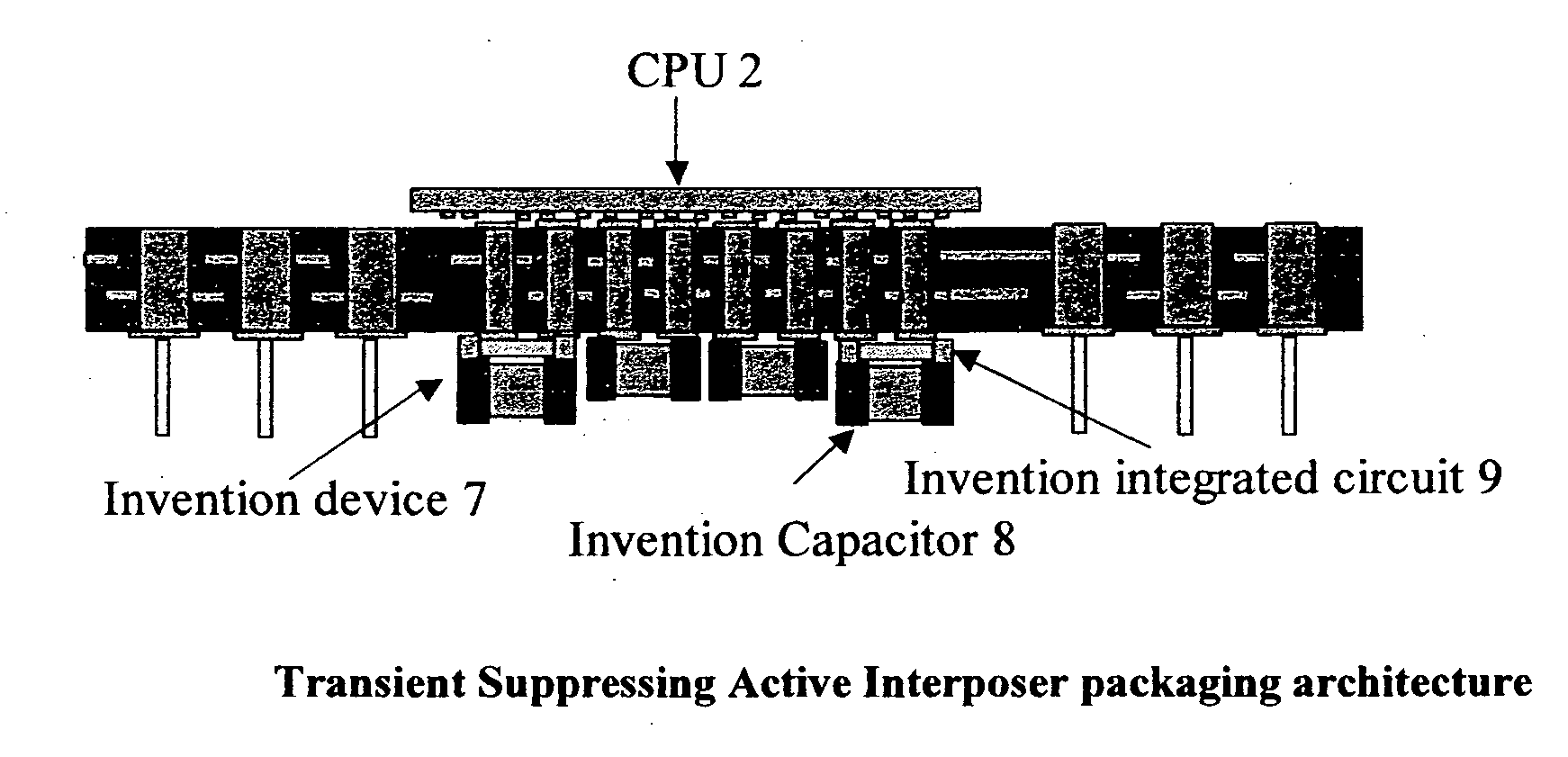
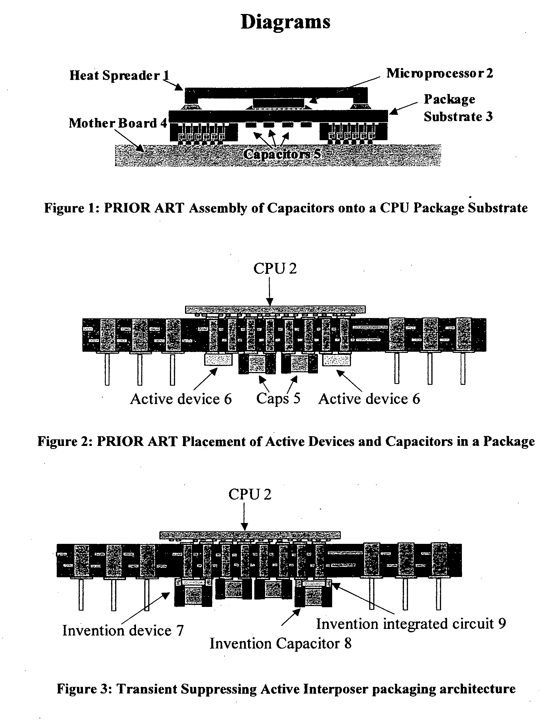
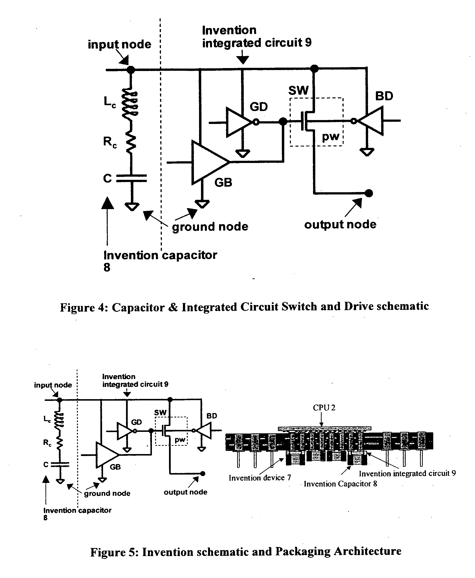
[0015]FIG. 3 illustrates the invention packaging architecture. This architecture is advantageous in two distinct ways. Firstly, it does not displace any of the existing capacitors as compared with the prior art. Second, it amplifies the charge storage capability in some of the capacitors through the isolation provided between capacitors dedicated to active noise suppression and the CPU power grid, which enables the use of a substantially higher voltage for charge storage on the dedicated capacitors.

[0016] The active interposer component of the invention architecture comprises of electronic circuits that sense noise on the CPU power grid or obtain signals from the CPU about impending changes of state, such as transition to it's ‘active’ state from a ‘standby’ state. Based on this information gathered, the circuits activate either high-voltage tolerant switches, or fast voltage regulators such as linear regulators enabling high current flow into the CPU power grid at the required ins...


PUM


Abstract

The invention proposes an interposer assembly architecture for noise suppression circuits on the package of a CPU or high power, high frequency VLSI device. In this architecture, charge is stored on dedicated capacitors at a voltage substantially higher than the operating voltage of the VLSI device. These capacitors are mounted upon active circuits that are packaged to match the size and form factor of the capacitors and this assembly is then attached to the package substrate. Charge is conveyed from the capacitor terminals on the backside of the packaged active circuits chip. Depending upon the capacitor construction, these terminals may either be double-sided contact terminals along the edge of the active device's package, or may be feed-through contacts. The active device attaches to the package substrate through both edge terminals and terminals built-up on the surface of the chip, increasing it's number of electrical pathways into the package substrate, matching the package substrate interconnect and reducing the electrical impedance of the charge flow path. The circuits within the active device may be any combination of semiconductor switches and/or voltage regulators, and may also contain voltage and current sensing circuitry.

Description

CROSS-REFERENCE TO RELATED DOCUMENTATION [0001] This application relates to USPTO DD 554540 dated the 31st of May 2004, entitled “Transient Suppressing Active Interposer”.TECHNICAL FIELD OF THE INVENTION [0002] Embodiments of the invention relate to electronic circuitry commonly employed to provide regulated voltages to other electronic, electromechanical or electro-optic devices and systems. Such circuitry falls under the broad category of power delivery management electronics. BACKGROUND & PRIOR ART [0003] Capacitors are commonly employed in electronic systems to store charge and minimize voltage excursions caused by fast load current variations. In order to maximize capacitor effectiveness, these devices are often physically placed at very close proximity to load devices. An example of such placement is the attachment of capacitors to the package substrate of microprocessors (CPU's) wherein the capacitors are mounted on the opposite side of the substrate, facing the processor chi...

Claims


Application Information

Patent Timeline
IPC IPC(8): G06F1/26H01L23/48H01L23/498H01L23/50H01L23/538H01L25/16
CPCG06F1/26H01L2224/16235H01L23/50H01L23/5384H01L25/16H01L2224/16H01L2224/73253H01L2924/15312H01L2924/1532H01L2924/16152H01L2924/19106H01L2924/3011H01L23/49811H01L2924/13091
Inventor NAIR, RAJENDRAN
Owner NAIR RAJENDRAN
Why Eureka
Try Eureka