Fully Cu-metallized III-V group compound semiconductor device with palladium/germanium/copper ohmic contact system

a technology of iiiv group and contact system, which is applied in the direction of semiconductor devices, semiconductor device details, electrical apparatus, etc., can solve the problems of indistinct contact border, too large extension of contact resistance, and inability to meet the requirements so as to promote the performance of iii-v group compound semiconductor devices and reduce electric impedance , the effect of reducing fabrication cos

Inactive Publication Date: 2009-08-06
NAT CHIAO TUNG UNIV
View PDF7 Cites 9 Cited by
  • Summary
  • Abstract
  • Description
  • Claims
  • Application Information

AI Technical Summary

Benefits of technology

[0009]Another objective of the present invention is provide a fully Cu-metallized III-V group compound semiconductor device with palladium / germanium / copper ohmic contact system to greatly reduce the fabrication cost of a III-V group compound semiconductor device and effectively promote the performance of a III-V group compound semiconductor device.
[0010]Further objective of the present invention is provide an fully Cu-metallized III-V group compound semiconductor device with palladium / germanium / copper ohmic contact system, wherein copper is used to reduce electric impedance and promote heat-dissipation effect.

Problems solved by technology

However, the gold / germanium / nickel ohmic contact metal layer has many weaknesses, such as too great an extension of the contact resistance, the indistinct contact border, and too high an annealing temperature.
Thus, the problems of using gold in ohmic contact metal layers still persist.

Method used


Image

  • Fully Cu-metallized III-V group compound semiconductor device with palladium/germanium/copper ohmic contact system
  • Fully Cu-metallized III-V group compound semiconductor device with palladium/germanium/copper ohmic contact system
  • Fully Cu-metallized III-V group compound semiconductor device with palladium/germanium/copper ohmic contact system

Examples


Embodiment Construction

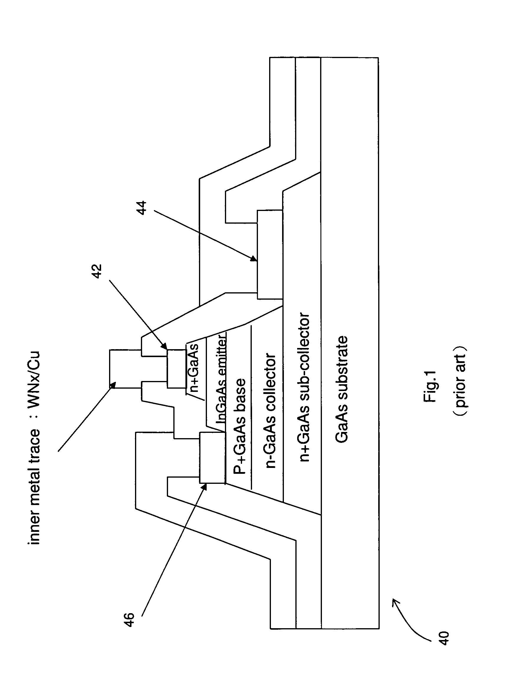
[0015]The spirit of the present invention is to propose device constituents to overall realize copper ohmic contact metal layers and copper interconnect metals in III-V group compound semiconductor devices, such as HBT, HEMT and MESFET. Below, the embodiment of the copper metallization in an InGaP—GaAs HBT is used to exemplify the present invention. However, the present invention is not limited to the embodiment.

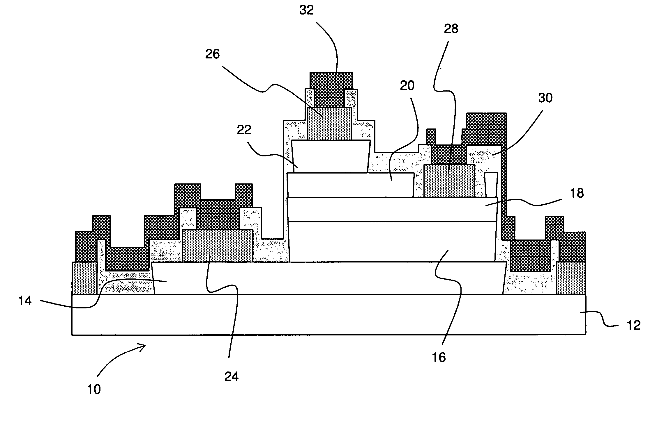
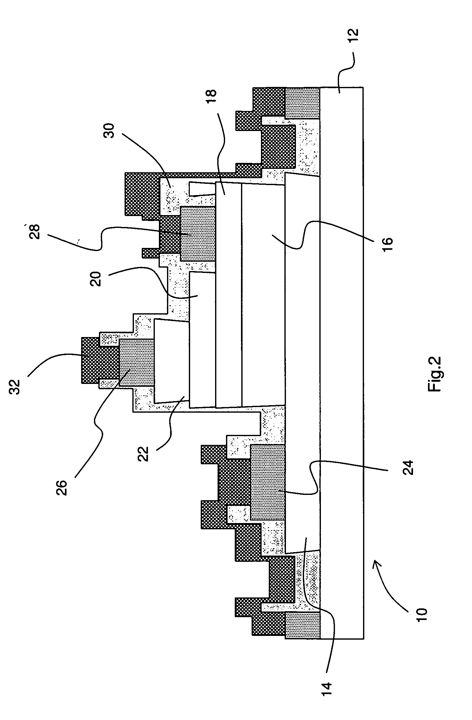
[0016]Refer to FIG. 2 a diagram schematically showing the structure of a fully Cu-metallized III-V group compound semiconductor device with palladium / germanium / copper ohmic contact system according to the present invention, wherein an InGaP—GaAs HBT is used to exemplify the structure thereof. The compound semiconductor device 10 comprises: a GaAs (Gallium Arsenide) substrate 12, an n+-GaAs collector 14, an n−-GaAs sub-collector 16, a p+-GaAs base 18, an n−-InGaP emitter 20 and a GaAs cap layer 22, wherein the n+-GaAs collector 14, n−-GaAs sub-collector 16, p+-GaAs base 18, n...


PUM

PropertyMeasurementUnit
temperatureaaaaaaaaaa
semiconductoraaaaaaaaaa

Abstract

The present invention discloses a fully Cu-metallized III-V group compound semiconductor device, wherein the fully Cu-metallized of a III-V group compound semiconductor device is realized via using an N-type gallium arsenide ohmic contact metal layer formed of a palladium / germanium / copper composite metal layer, a P-type gallium arsenide ohmic contact metal layer formed of a platinum / titanium / platinum / copper composite metal layer, and interconnect metals formed of a titanium / platinum / copper composite metal layer. Thereby, the fabrication cost of III-V group compound semiconductor devices can be greatly reduced, and the performance of III-V group compound semiconductor devices can be greatly promoted. Besides, the heat-dissipation effect can also be increased, and the electric impedance can also be reduced.

Description

BACKGROUND OF THE INVENTION[0001]1. Field of the Invention[0002]The present invention relates to a III-V group compound semiconductor element, particularly to a fully Cu-metallized III-V group compound semiconductor device with palladium / germanium / copper ohmic contact system.[0003]2. Description of the Related Art[0004]Traditional III-V group semiconductor elements, such as HBT (Heterojunction Bipolar Transistor), HEMT (High Electron Mobility Transistor) and MESFET (Metal Semiconductor Field Effect Transistor), adopt a gold / germanium / nickel composite layer as the ohmic contact metal layer and adopt gold as the material of interconnect metals. However, the gold / germanium / nickel ohmic contact metal layer has many weaknesses, such as too great an extension of the contact resistance, the indistinct contact border, and too high an annealing temperature.[0005]In consideration of the RC delay effect, the elements can attain better performance via replacing gold with copper, which has lower...

Claims


Application Information

Patent Timeline
Patent Type & Authority Applications(United States)
IPC IPC(8): H01L29/732
CPCH01L23/53238H01L29/452H01L2924/3011H01L29/7371H01L29/475H01L2924/0002H01L2924/00
Inventor CHANG, EDWARD YICHEN, KE-SHIAN
Owner NAT CHIAO TUNG UNIV
Why Eureka
Try Eureka