

Oxide semiconductor thin film transistor and preparing method thereof
A technology of oxide semiconductors and thin film transistors, applied in the direction of transistors, semiconductor devices, electrical components, etc., can solve the problems of disconnection or electrical subcritical swing S.S., erosion, etc., to reduce the number of photomasks, reduce the The effect of production costs
- Summary
- Abstract
- Description
- Claims
- Application Information
AI Technical Summary
Problems solved by technology
Method used
Image

Examples
Embodiment Construction
[0033] In order for those skilled in the art to have a better understanding of the present invention, preferred embodiments of the present invention are enumerated below, together with the accompanying drawings, to describe in detail the composition and desired effects of the present invention.
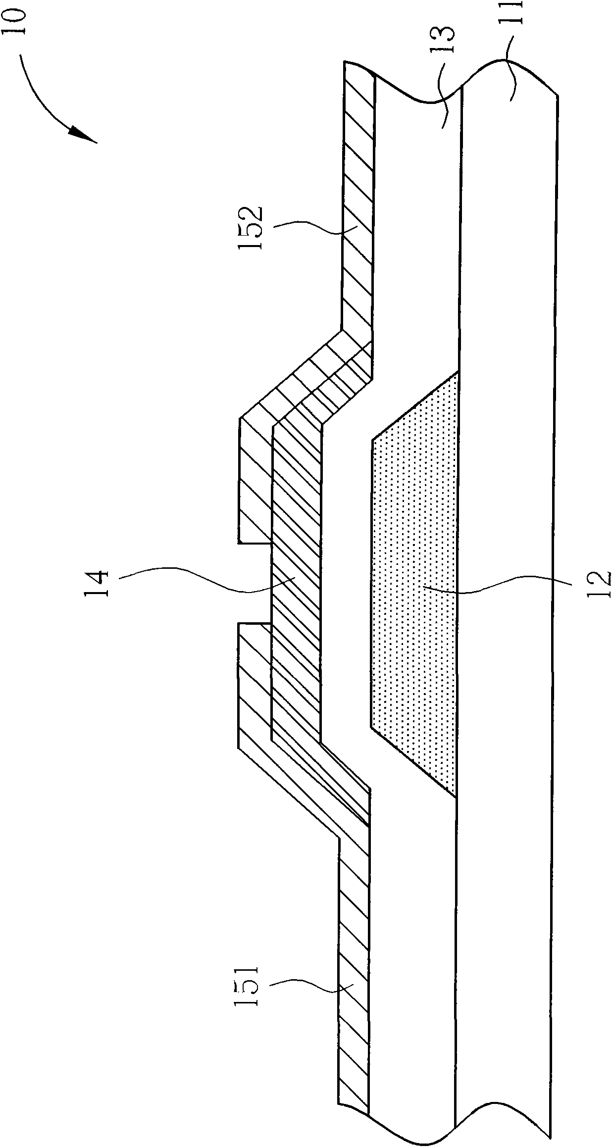
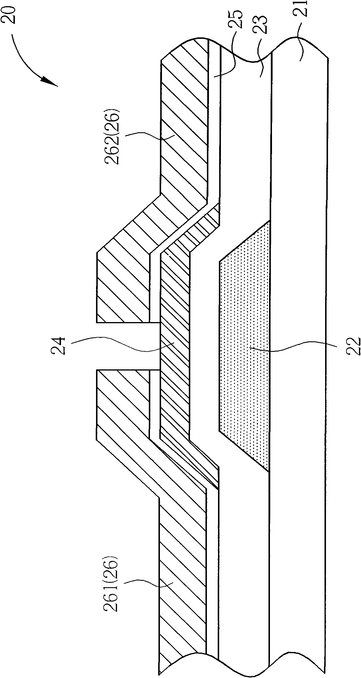
[0034] Please refer to figure 2 , figure 2 A schematic cross-sectional view of a preferred embodiment of the present invention is shown. Such as figure 2 As shown, the oxide thin film transistor structure 20 of this embodiment includes a substrate 21, a gate 22 disposed on the substrate 21, a semiconductor insulating layer 23 disposed on the substrate 21 and the gate 22, and an oxide semiconductor layer 24 disposed On the semiconductor insulating layer 23, a patterned semiconductor layer 25 is disposed on the oxide semiconductor layer 24, a source 261 and a drain 262 are respectively disposed on the patterned semiconductor layer 25, and the source 261 and the drain 262 are A met...
PUM
 Abstract
Description
Claims
Application Information