Semiconductor structure and method for manufacturing same

A manufacturing method, semiconductor technology, applied in semiconductor/solid-state device manufacturing, semiconductor devices, semiconductor/solid-state device components, etc.

Inactive Publication Date: 2011-02-02
NIKO SEMICON
View PDF0 Cites 0 Cited by
  • Summary
  • Abstract
  • Description
  • Claims
  • Application Information

AI Technical Summary

Problems solved by technology

[0008] The purpose of the present invention is to overcome the defects of existing semiconductor structures and manufacturing methods thereof, and provide a semiconductor structure of a novel structure and manufacturing methods thereof. The technical problem to be solved is to make it utilize the formation of oxide layers while, Part of the oxide layer separates the space or provides a height difference for the conductive line (Bus) to be formed on the

Method used


Image

  • Semiconductor structure and method for manufacturing same
  • Semiconductor structure and method for manufacturing same
  • Semiconductor structure and method for manufacturing same

Examples


Embodiment Construction

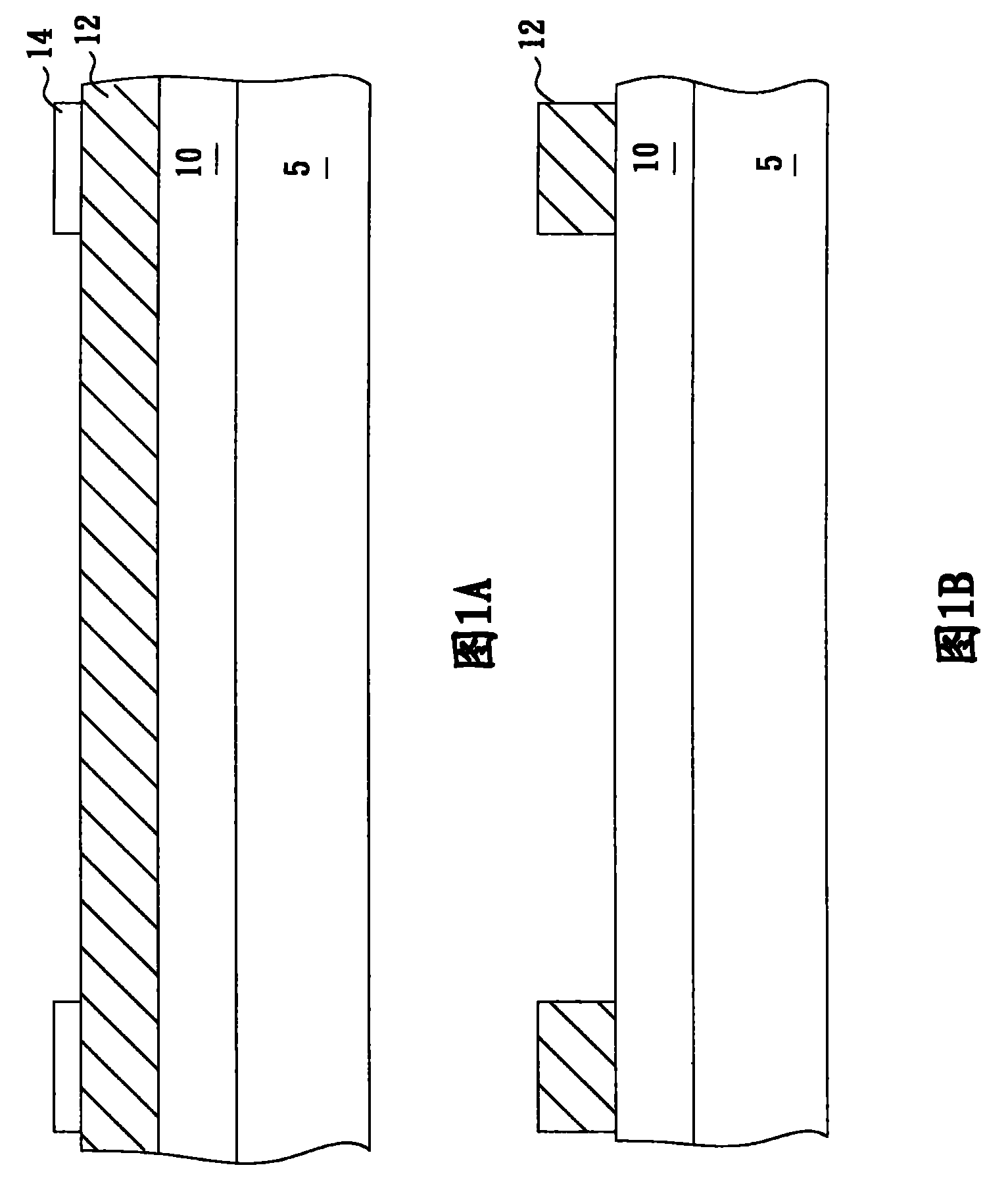
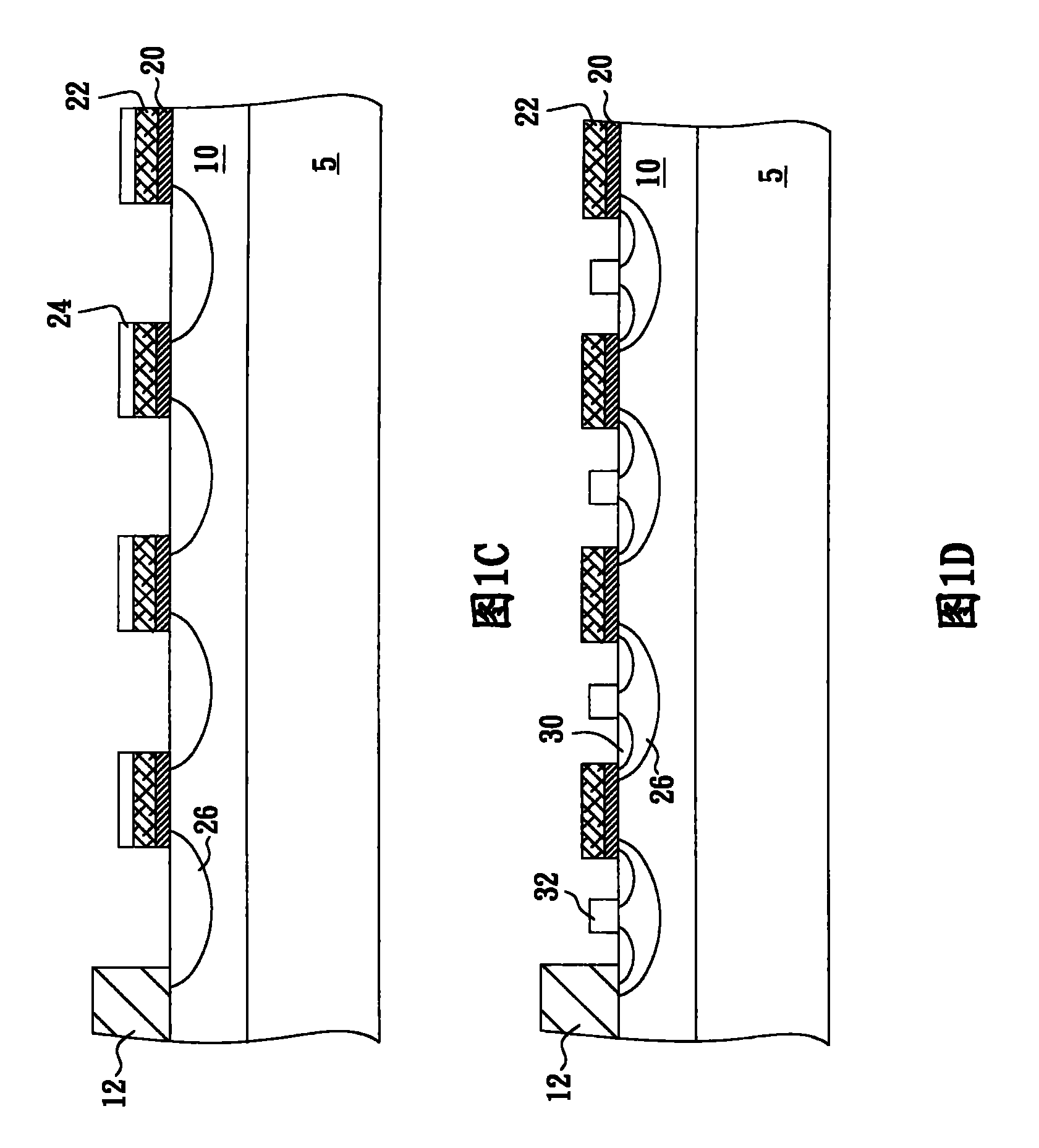
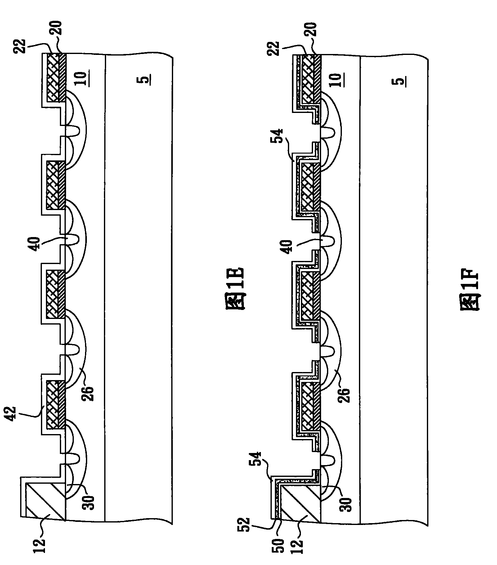
[0092]In order to further explain the technical means and effects that the present invention adopts to achieve the intended purpose of the invention, below in conjunction with the accompanying drawings and preferred embodiments, the specific implementation, structure, steps, Features and their functions are described in detail below.

[0093] The spirit of the present invention is to use the process of forming a non-conductive material (such as: field oxide or silicon dioxide, etc.) , such as: Gate Bus Line, Data Line, etc., are used as the transmission of control signals, electrically connected to the various operating units in the operating area of ​​the integrated circuit, and transmit the control signals to these operating units for use It operates according to this control signal. The non-conductive material used as the auxiliary part will partition a plurality of spaces, so that the conductive material formed on it will fill these spaces. In this way, when etching remo...


PUM


Abstract

The invention relates to a semiconductor structure and a method for manufacturing the same. The method for manufacturing a semiconductor forms an oxide layer, and at the same time, partial oxide layer areas separate space or provide height difference so as to enable a conduction bus (Bus) to be formed on the partial oxide layer areas. Therefore, the conduction bus can be defined without needing additional photomasks and can form conduction materials on the oxide layer areas in the subsequent process of manufacturing. Therefore, the manufacturing of the semiconductor can reduce the number of required photomasks so as to reduce cost.

Description

technical field [0001] The present invention relates to a semiconductor structure and its method, in particular to a double diffused metal oxide semiconductor power transistor (DMOS) structure and its method with a guard ring. Background technique [0002] While the functions of today's integrated circuits are becoming more and more powerful, their structures are also becoming more and more complex, resulting in an increase in the number of photomasks (photomasks are photomasks, which are referred to as photomasks in this article) of integrated circuits, and the cost Also rising. [0003] see here Figure 1A to Figure 1I , taking the manufacturing of N-type double-diffused metal oxide semiconductor power transistors (the manufacturing process is the manufacturing process, which is referred to as manufacturing herein) as an example to illustrate. refer to Figure 1A growing an N- epitaxial layer 10 and a field region oxide 12 sequentially on the silicon substrate 5, and usi...

Claims


Application Information

Patent Timeline
Patent Type & Authority Patents(China)
IPC IPC(8): H01L27/02H01L27/088H01L23/522H01L21/8234H01L21/768
Inventor 涂高维董正晖
Owner NIKO SEMICON
Why Eureka
Try Eureka