Producing method for thin-film transistor array baseplate

A technology of thin-film transistors and array substrates, which is applied in the field of manufacturing thin-film transistor array substrates, can solve the problems of reduced yield and production capacity, and achieve the effect of reducing production costs and the number of photomasks

Inactive Publication Date: 2007-08-22
AU OPTRONICS CORP
View PDF7 Cites 1 Cited by
  • Summary
  • Abstract
  • Description
  • Claims
  • Application Information

AI Technical Summary

Problems solved by technology

[0004] However, with the development trend of TFT-LCD toward large-scale production, many problems and challenges will be faced, such as lower good rate and lower production capacity, etc.

Method used


Image

  • Producing method for thin-film transistor array baseplate
  • Producing method for thin-film transistor array baseplate
  • Producing method for thin-film transistor array baseplate

Examples


no. 1 example

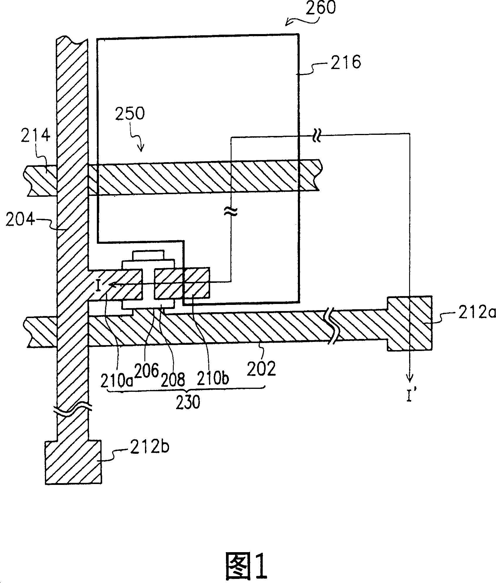
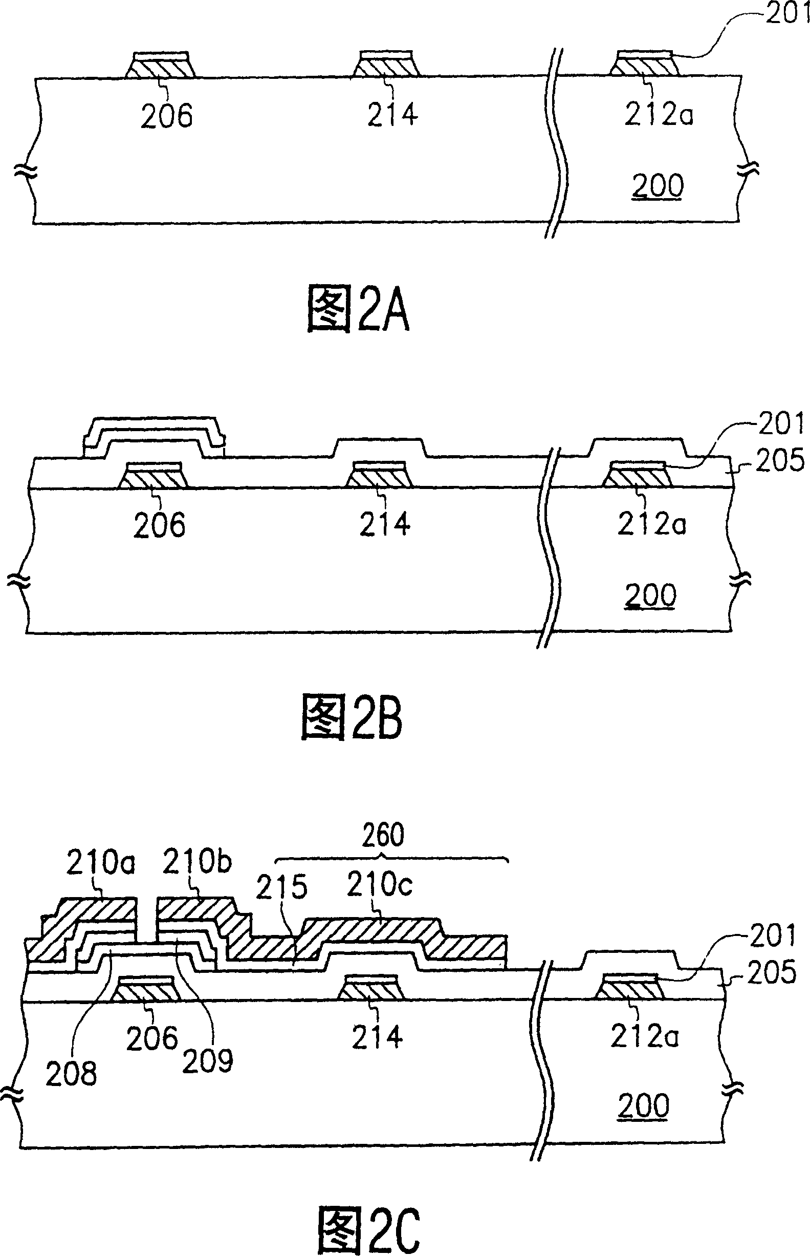
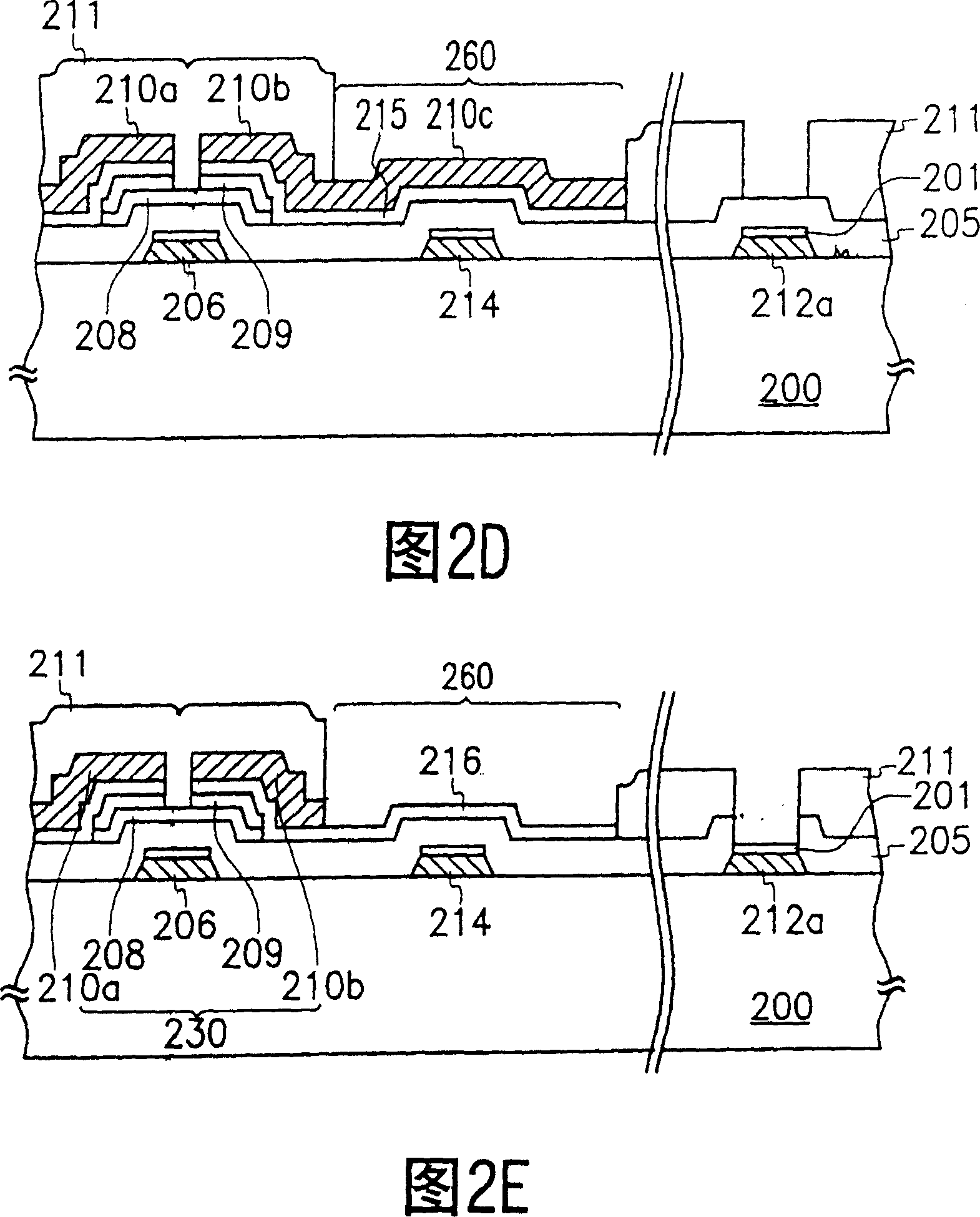
[0046] As shown in FIG. 1, it is a schematic top view of a thin film transistor array substrate according to a preferred embodiment of the present invention; as shown in FIGS. 2A to 2E, it is a thin film transistor array according to a preferred embodiment of the present invention. The schematic cross-sectional view of the manufacturing process of the substrate is a schematic cross-sectional view from I-I in FIG. 1 .

[0047] Please refer to FIG. 1 and FIG. 2A at the same time. Firstly, a substrate 200 is provided, wherein the substrate 200 is, for example, a glass substrate or a plastic substrate. Afterwards, a first metal layer (M1) (not shown) is formed on the substrate 200, and a first photomask manufacturing process is performed to define the gate 206 and the scanning wiring electrically connected to the gate 206 202 , a common line 214 parallel to the scanning wiring 202 and a first terminal portion 212 a formed at an edge of the substrate 200 . Wherein, the first termi...

no. 2 example

[0058] 3A to FIG. 3N are schematic cross-sectional views of a manufacturing process of a thin film transistor array substrate according to another preferred embodiment of the present invention, which are schematic cross-sectional views taken from I-I' in FIG. 1 .

[0059] Please refer to FIG. 1 and FIG. 3A at the same time. First, a first metal layer (M1) (not shown) is formed on the substrate 200, and the first photomask manufacturing process is performed to define the gate 206 and the gate 206. The scanning wiring 202 electrically connected, the common line 214 parallel to the scanning wiring 202 and the first terminal portion 212 a formed at two edges of the substrate 200 . Wherein, the first terminal portion 212a is electrically connected to the scanning wiring 202, and is subsequently used to electrically connect to the driving circuit, and the common line 214 is subsequently used as the lower electrode of the pixel storage capacitor 250. In a preferred implementation In ...


PUM


Abstract

A method for manufacturing TFT array substrate is carried out by: forming a grid and a scanning wire connected with the grid, forming a grid isolative layer, forming a channel layer on the isolative layer, forming a transparent layer and a metal layer above the substrate to be patterned to define source / drain and data wires and picture elements zones, forming a protective layer with metal layer of the picture element zone opened, finally, eliminating the latter metal layer with the latter protective layer as mask to form element electrodes. It reduces cost due to four optical masks needed only.

Description

technical field [0001] The present invention relates to a manufacturing method of a thin film transistor array (Thin Film Transistor Array) substrate, and in particular to a manufacturing method of a thin film transistor array substrate capable of reducing the number of photomasks. Background technique [0002] The thin film transistor liquid crystal display is mainly composed of a thin film transistor array substrate, a color filter array substrate and a liquid crystal layer, wherein the thin film transistor array substrate is composed of a plurality of thin film transistors arranged in an array and a pixel electrode ( PixelElectrode) to form several pixel structures. The above-mentioned thin film transistor includes a gate, a channel layer, a drain and a source, and is used as a switch element of a liquid crystal display unit. [0003] Among the known manufacturing processes of thin film transistors, a five-pass photomask manufacturing process is more common. Wherein, th...

Claims


Application Information

Patent Timeline
Patent Type & Authority Patents(China)
IPC IPC(8): H01L21/00H01L21/336H01L21/84H01L29/786G02F1/136
Inventor 杨克勤
Owner AU OPTRONICS CORP
Why Eureka
Try Eureka