Film encapsulation method

A thin film encapsulation and thin film technology, which is applied in thin material processing, transportation and packaging, gaseous chemical plating, etc., can solve the problems of many operation steps, damage to the organic layer of the device, and long processing cycle, so as to simplify the operation steps and shorten the processing The cycle and the effect of reducing equipment cost

Inactive Publication Date: 2010-04-21
SUZHOU INST OF NANO TECH & NANO BIONICS CHINESE ACEDEMY OF SCI
View PDF0 Cites 45 Cited by
  • Summary
  • Abstract
  • Description
  • Claims
  • Application Information

AI Technical Summary

Problems solved by technology

The disadvantage of this method is that it needs to be completed by different methods in two processing chambers, with many operating steps and a long processing cycle; and commonly used methods such as PVD, CVD, high vacuum thermal deposition, and magnetron sputtering grow SiO x or SiN x The thin film requires a higher temperature, and the high temperature will damage the organic layer of the device to a certain extent

Method used


Image

  • Film encapsulation method
  • Film encapsulation method
  • Film encapsulation method

Examples


Embodiment 1

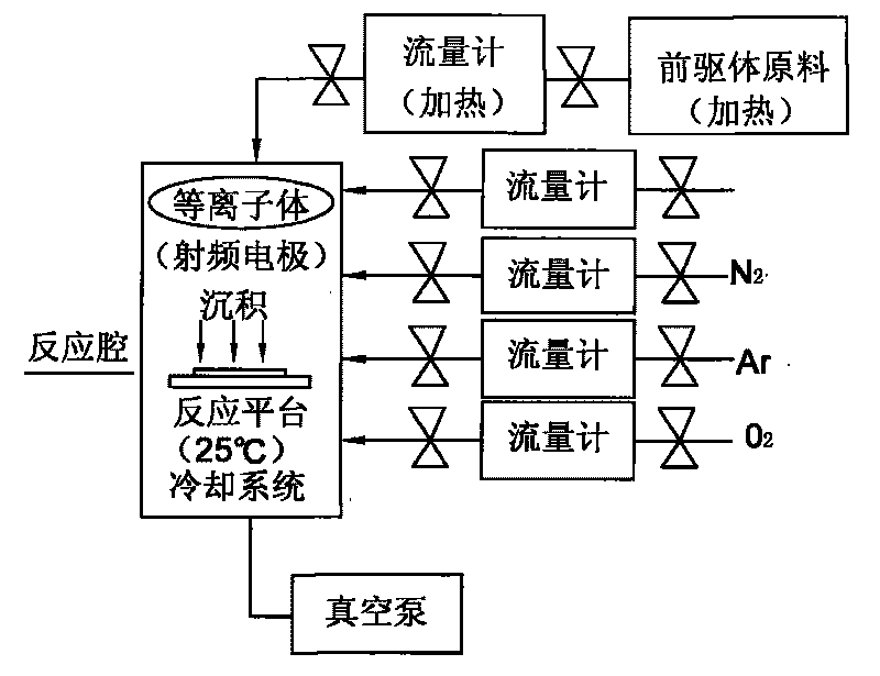
[0038] After the preparation of the OLED device is completed, a CuPc protective film of about 100nm is vacuum-deposited on the aluminum metal electrode of the device so that the device will not be damaged during the packaging process, and then the OLED device is transferred to the PECVD (PECVD) for packaging under an inert atmosphere. Such as figure 1 ) cavity, the cavity is about 200 mm in diameter and 200 mm in height, and the device is placed on the substrate tray facing up, and the area and area of ​​the package are controlled by a mask. Vacuum the cavity to 1.5Pa, pass through hexamethyldisiloxane (HMDSO), adjust the radio frequency intensity to 60mA under the plasma (microwave electron cyclotron resonance (ERC), frequency 40KHz), and realize it under the condition of Ar carrier gas For the growth of the organic silicon polymer film, the growth time is one minute, and the pressure in the chamber is 6Pa during the growth. Then turn off the plasma source, stop feeding argo...

Embodiment 2

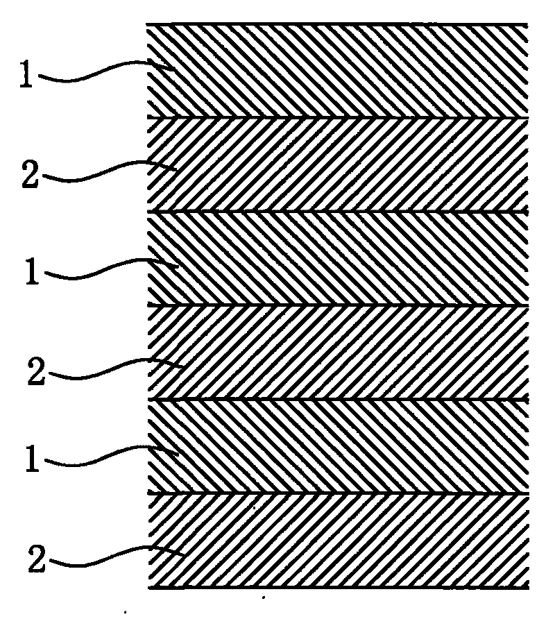
[0040] The Alq3 OLED device prepared on the ITO glass substrate that adopts the method described in embodiment one to package, carries out test and characterization, and carries out the comparison of device life-span, efficiency with traditional glass cover epoxy resin encapsulation, the result finds: this method encapsulation device and Devices without any encapsulation are equivalent in efficiency, indicating that the encapsulation has no damage to the device. If the CuPc layer is not deposited before OLED encapsulation, there will be a small amount of damage; in the life test, the life of the glass encapsulation device is 3000 hours, and the encapsulation device of the present invention More than 3000 hours, it shows that the barrier ability of the present invention to water and oxygen is basically equal to that of epoxy resin encapsulation with glass cover.

Embodiment 3

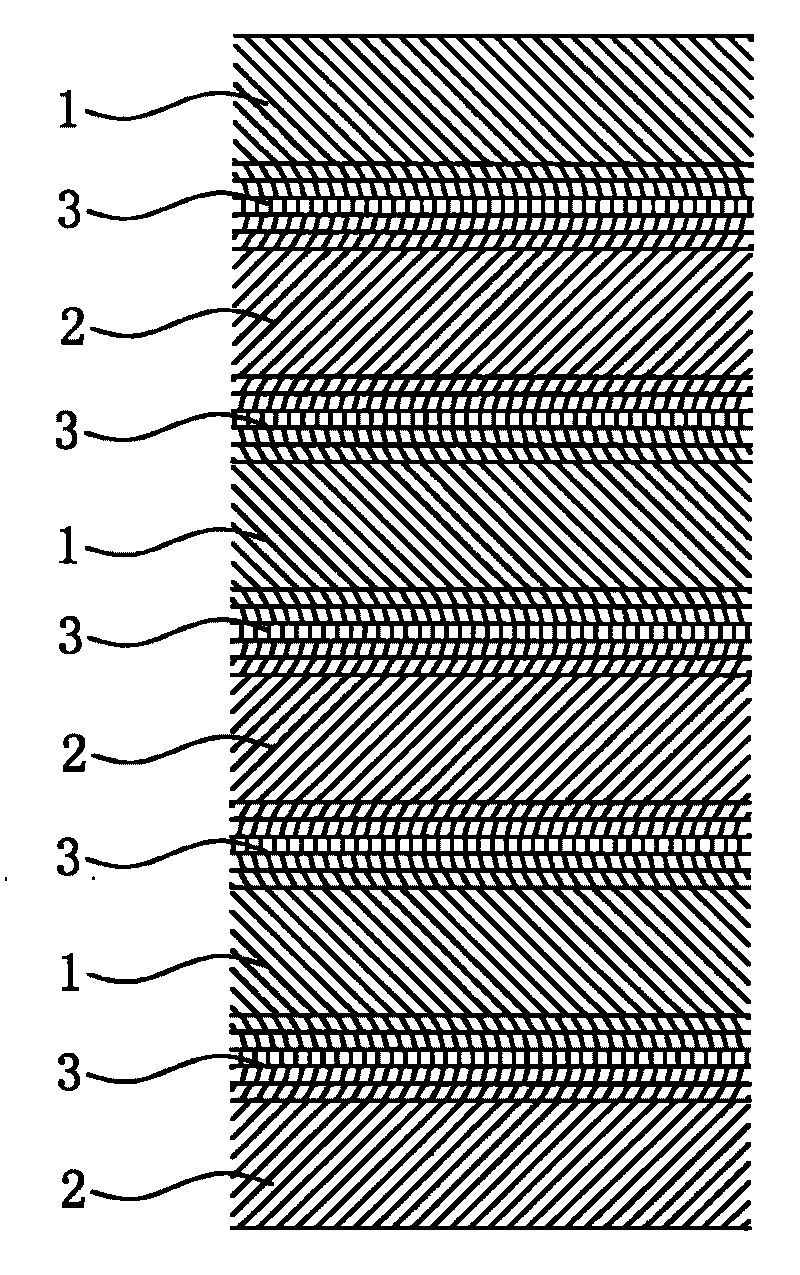
[0042] After the preparation of the OLED device is completed, a CuPc protective film of about 100nm is vacuum-deposited on the aluminum metal electrode of the device to prevent the device from being damaged during the packaging process, and then the OLED device is transferred to the PECVD chamber for packaging in an inert atmosphere In the body, and use a mask to control the area and area of ​​the package. At the same time, a thin steel sheet with a thickness of 1 micron is placed next to the device, so that the same packaging film grows on the steel sheet while the device is packaged. Vacuum the cavity to 1.5Pa, pass through hexamethyldisiloxane (HMDSO), adjust the radio frequency intensity to 60mA under plasma (microwave electron cyclotron resonance (ERC), frequency 40KHz), and adjust the radio frequency intensity to 60mA in NH 3 The growth of the silicon nitride film is realized under the condition of the carrier gas, the growth time is one minute, and the pressure in the c...


PUM

PropertyMeasurementUnit
thicknessaaaaaaaaaa
thicknessaaaaaaaaaa
thicknessaaaaaaaaaa

Abstract

The invention discloses a film encapsulation method, which adopts a PECVD method and a mode of growing a film on the surface of a device to separate the device from water and oxygen in the air and achieve the aim of physical protection so as to implement encapsulation for the device. The method specifically comprises the following steps: (1) placing the device to be encapsulated into a PECVD device, and setting a mask plate to control the encapsulated area; and (2) using an organic silicon precursor and adopting the PECVD method to deposit an inorganic layer, a polymer layer or a transition layer under the condition of plasma to obtain the required encapsulation structure. The method can finish the preparation of the polymer layer, the inorganic layer and the transition layer in one reaction cavity by adopting the PECVD method so as to simplify the operation steps, reduce the cost and shorten the period; and meanwhile, the prepared encapsulation layer has a transition layer structure of a large amount of polymer or component gradually changed to silicon oxide or silicon nitride from soft polymer, so the encapsulation layer has enough flexibility and is not influenced by interface problem.

Description

[0001] The invention relates to a device packaging film structure and a packaging method thereof, in particular to a packaging structure and a packaging method of a display, a diode, a micro-electromechanical sensor device, an organic electroluminescent device (OLED), and the like. Background technique [0002] For most devices, such as displays, diodes, MEMS sensing devices, etc., a completely hermetic physical package is required for protection. [0003] Studies have shown that components such as water vapor and oxygen in the air have a great impact on the life of OLEDs. The reasons are mainly considered from the following aspects: when OLED devices work, electrons are injected from the cathode, which requires that the cathode work function be as low as possible, but These metals used as cathodes, such as aluminum, magnesium, calcium, etc., are generally more active and easily react with the infiltrated water vapor. In addition, water vapor can also chemically react with the...

Claims


Application Information

Patent Timeline
Patent Type & Authority Applications(China)
IPC IPC(8): H01L21/56H01L21/312H01L21/314H01L23/31H01L23/29H01L51/56H01L51/52
CPCH01L2251/5346C23C16/029H01L51/5237C23C16/042C23C16/401H01L23/293H01L2924/0002Y10T428/23H10K50/8445H10K2101/80H01L2924/00
Inventor 李丰苏文明
Owner SUZHOU INST OF NANO TECH & NANO BIONICS CHINESE ACEDEMY OF SCI
Why Eureka
Try Eureka