Method for producing semiconductor structure of thin-film transistor and planar display device

A technology of thin-film transistors and manufacturing methods, applied in semiconductor/solid-state device manufacturing, optics, instruments, etc., can solve the problems of expensive photomasks, high cost, and increased manufacturing time, so as to reduce the cost of photomasks and reduce Production cost, effect of reducing the number of photomasks

Active Publication Date: 2007-11-21
AU OPTRONICS CORP
View PDF0 Cites 0 Cited by
  • Summary
  • Abstract
  • Description
  • Claims
  • Application Information

AI Technical Summary

Problems solved by technology

However, it is well known that photomasks are expensive. The more photomasks, the higher the cost. In addition, the manufacturing time will increase. How to reduce the number of photomasks can not only reduce the cost In addition, it can also accelerate the output speed and increase the competitiveness of products

Method used


Image

  • Method for producing semiconductor structure of thin-film transistor and planar display device
  • Method for producing semiconductor structure of thin-film transistor and planar display device
  • Method for producing semiconductor structure of thin-film transistor and planar display device

Examples


Embodiment Construction

[0051] The invention effectively reduces the number of photomasks needed in the process of manufacturing the thin film transistor of the liquid crystal display, and can effectively reduce the manufacturing cost of the liquid crystal display. The following will clearly illustrate the spirit of the present invention with illustrations and detailed descriptions. After those skilled in the art understand the preferred embodiments of the present invention, they can be changed and modified by the techniques taught in the present invention without departing from the present invention. The spirit and scope of the invention.

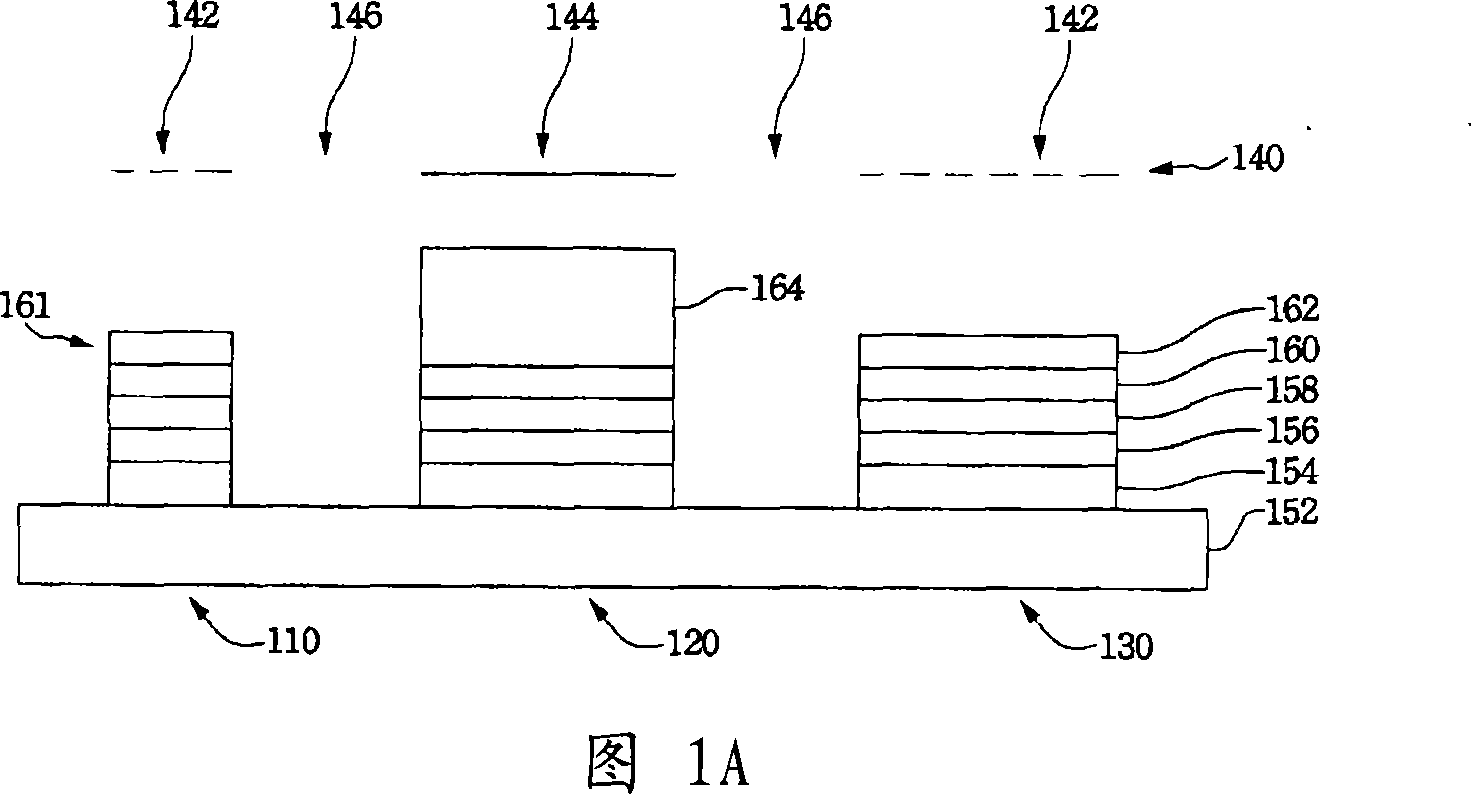
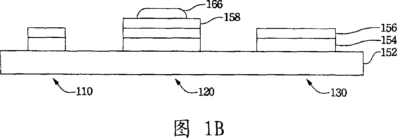
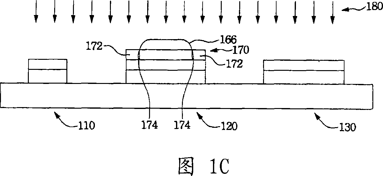
[0052] 1A-1H are schematic diagrams illustrating the fabrication process of a preferred embodiment of the fabrication method of the thin film transistor structure of the present invention. Referring first to FIG. 1A , a substrate 152 is provided, and then a conductive layer 154 , a dielectric layer 156 , a channel layer 158 , a passivation layer 160 and a photore...


PUM

PropertyMeasurementUnit
thicknessaaaaaaaaaa

Abstract

The production method for film transistor includes: forming layers in order on the base plate of the premier conducting, the premier dielectric, groove, protection and the premier anti-light etching; then removing the outer ring parts of the premier anti-light etching layer and the protection layer as well as parts of the groove layer; removing all anti-light etching layer; forming interval wall on the side wall of the premier conducting layer and the premier dielectric layer and linking the groove layer; removing the exposed groove layer masked by the patterned protection layer.

Description

technical field [0001] The invention relates to a manufacturing method of a thin film transistor structure, in particular to a manufacturing method of a thin film transistor structure of a liquid crystal display panel. Background technique [0002] In recent years, optoelectronic-related technologies have been continuously introduced, coupled with the arrival of the digital age, which has further promoted the vigorous development of the liquid crystal display market. Liquid crystal displays have the advantages of high image quality, small size, light weight, low driving voltage, and low power consumption, so they are widely used in personal digital assistants (PDAs), mobile phones, video recorders, notebook computers, desktops, etc. Consumer communication or electronic products such as upper-type displays, car displays, and projection TVs are gradually replacing cathode ray tubes and becoming the mainstream of displays. [0003] Liquid Crystal Display (LCD) is a display dev...

Claims


Application Information

Patent Timeline
Patent Type & Authority Applications(China)
IPC IPC(8): H01L21/336H01L21/84G02F1/1362
Inventor 陈昱丞
Owner AU OPTRONICS CORP
Why Eureka
Try Eureka