Semiconductor device structure

a technology of semiconductor devices and devices, applied in the direction of semiconductor devices, basic electric elements, electrical equipment, etc., can solve the problems of sgoi substrates that have limited performance of devices, complicating silicon layers that may also complicate or affecting the performance of devices built, etc., to achieve high ge composition, wide range of ge composition, and high ge composition

Inactive Publication Date: 2005-09-06
MASSACHUSETTS INST OF TECH
View PDF297 Cites 69 Cited by
  • Summary
  • Abstract
  • Description
  • Claims
  • Application Information

AI Technical Summary

Benefits of technology

[0011]According to one aspect of the invention, the invention provides a method of semiconductor device fabrication, and more specifically, a method of production of a general semiconductor substrate of relaxed SGOI for various electronics or optoelectronics applications, a method of production of strained Si or strained SiGe FET devices on SGOI, and the production of monocrystalline III-V or II-VI material-on-insulator substrates. The invention provides a method of producing a relaxed Si1-xGex-on-insulator substrate with high Ge composition and wide range of Ge composition, and the Ge composition may be much less or much higher than 20%. The invention provides an improved method to fabricate strained-Si or strained-SiGe MOSFET devices on SGOI substrate with high Ge composition. When strained-Si n-MOSFETs are fabricated on relaxed Si1-xGex-on-insulators substrates with a high Ge composition, 25% for example, there is significant enhancement on electron mobility as compared to the co-processed bulk-Si MOSFETs on conventional bulk Si substrate.

Problems solved by technology

One of the main drawbacks is the quality of the resulting Si1-xGex film and the BOX layer.
Due to the low Ge composition, the device fabricated on those SGOI substrates has limited performance.
The silicon layer in the structure is unnecessary for an ideal SGOI structure, and may complicate or undermine the performance of devices built on it.
The presence of the silicon layer in the structure may be for the purpose of facilitating the wafer bonding process, but is unnecessary for ideal SGOI substrates.
Again, the silicon layer may also complicate or undermine the performance of devices built on it.
For example, it may form a parasitic back channel on this strained-Si, or may confine unwanted electrons due to the band gap offset between the Si and SiGe layer.
Moreover, the etch stop of p++ in the above structure is not practical when a first graded Si1-yGey layer has a final y value larger than 0.2.
Therefore, KOH will not be able to remove practically all of the first compositionally graded Si1-yGey layer (when y is larger than 0.2) and the second relaxed SiGe layer, thus using a p++ layer as an etch-stop for KOH is not practical.
Again, such a structure is not an ideal SGOI substrate and the silicon layer is unnecessary, and may complicate or undermine the performance of devices built on it.
However, as the Ge composition in the final SGOI structure is fixed by the etch-stop Si1-yGey, if the desired Ge composition in the final SGOI structure is much higher or lower than 0.2, the above method is not practical.

Method used


Image

  • Semiconductor device structure
  • Semiconductor device structure
  • Semiconductor device structure

Examples


Embodiment Construction

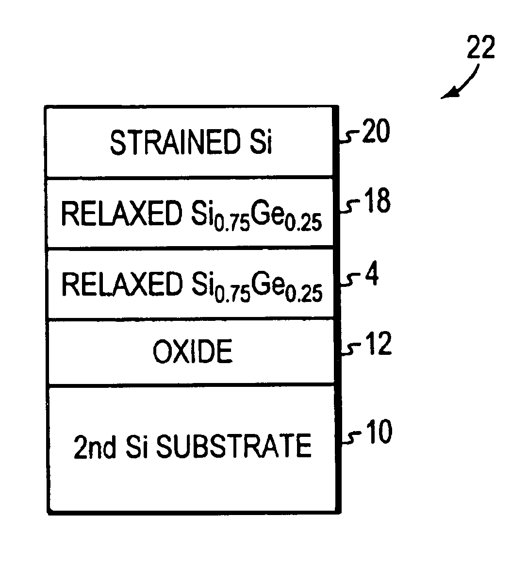
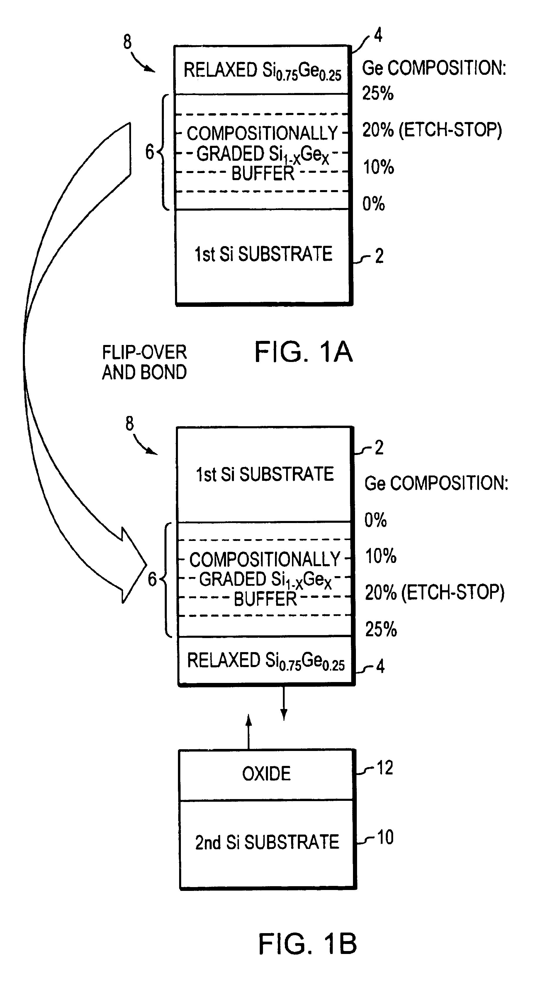
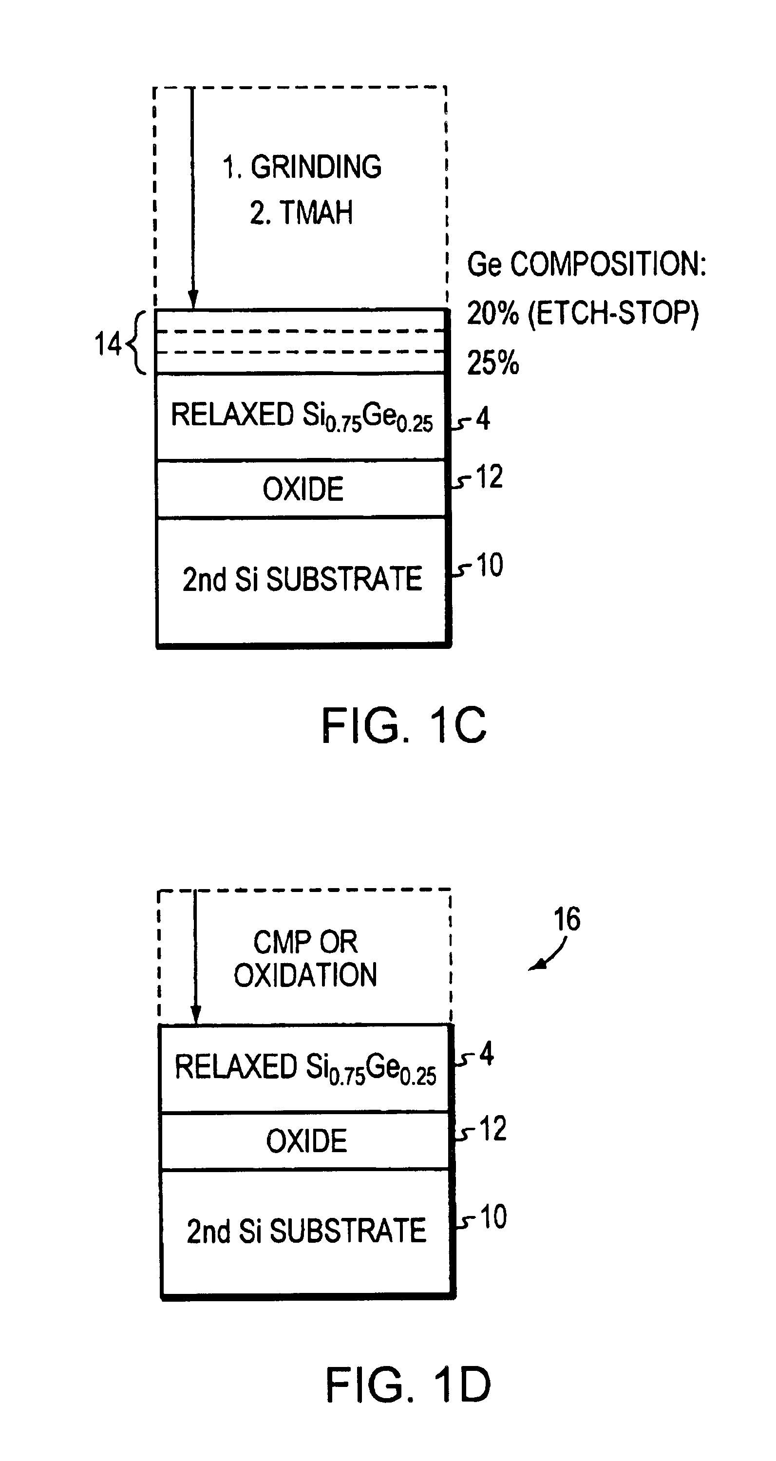
[0021]FIGS. 1(a)-1(d) are flow process diagrams of an experimental fabrication process of a SGOI substrate with Ge composition of 25% in accordance with one embodiment of the invention. Starting with a 4-inch Si (100) substrate 2, high quality relaxed Si0.75Ge0.25 layer 4 is grown at 900° C. by UHVCVD using a compositionally graded Si1-xGex buffer 6 technique as described in U.S. Pat. No. 5,221,413 issued to Brasen et al., which is incorporated herein by reference in its entirety. Using this technique, a compositionally graded Si1-xGex buffer 6 can be grown epitaxially on Si substrate, which allows a relaxed SiGe layer to be grown on the top of the buffer with low threading dislocation density.

[0022]FIG. 2. is a block diagram of a compositionally graded Si1-xGex buffer 30. The compositionally graded Si1-xGex buffer 30 is a multi-layer structure where the Ge composition in each layer is changing gradually from a beginning value to a final value. For example, the compositionally grade...


PUM


Abstract

A method of fabricating a semiconductor structure. According to one aspect of the invention, on a first semiconductor substrate, a first compositionally graded Si1-xGex buffer is deposited where the Ge composition x is increasing from about zero to a value less than about 20%. Then a first etch-stop Si1-yGey layer is deposited where the Ge composition y is larger than about 20% so that the layer is an effective etch-stop. A second etch-stop layer of strained Si is then grown. The deposited layer is bonded to a second substrate. After that the first substrate is removed to release said first etch-stop Si1-yGey layer. The remaining structure is then removed in another step to release the second etch-stop layer. According to another aspect of the invention, a semiconductor structure is provided. The structure has a layer in which semiconductor devices are to be formed. The semiconductor structure includes a substrate, an insulating layer, a relaxed SiGe layer where the Ge composition is larger than approximately 15%, and a device layer selected from a group consisting of, but not limited to, strained-Si, relaxed Si1-yGey layer, strained S1-zGez layer, Ge, GaAs, III-V materials, and II-VI materials, where Ge compositions y and z are values between 0 and 1.

Description

PRIORITY INFORMATION[0001]This application claims priority from provisional application Ser. No. 60 / 281,502 filed Apr. 4, 2001.BACKGROUND OF THE INVENTION[0002]The invention relates to the production of a general semiconductor substrate of relaxed Si1-xGex-on-insulator (SGOI) for various electronics or optoelectronics applications, the production of strained Si or strained SiGe field effect transistor (FET) devices on SGOI, and the production of monocrystalline III-V or II-VI material-on-insulator substrates.[0003]Relaxed SGOI is a very promising technology as it combines the benefits of two advanced technologies: the conventional SOI technology and the disruptive SiGe technology. The SOI configuration offers various advantages associated with the insulating substrate, namely reduced parasitic capacitances, improved isolation, reduced short-channel-effect, etc. The SiGe technology also has various advantages, such as mobility enhancement and integration with III-V devices.[0004]One ...

Claims


Application Information

Patent Timeline
Patent Type & Authority Patents(United States)
IPC IPC(8): H01L21/70H01L21/02H01L21/762H01L21/20H01L21/306
CPCH01L21/30608H01L21/76256H01L21/02381H01L21/0245H01L21/0251H01L21/02532H01L21/02664
Inventor CHENG, ZHIYUANFITZGERALD, EUGENE A.ANTONIADIS, DIMITRI A.
Owner MASSACHUSETTS INST OF TECH
Why Eureka
Try Eureka