Low Density Drain HEMTs

a drain hemts and low density technology, applied in the direction of basic electric elements, electrical apparatus, semiconductor devices, etc., can solve the problems of excessive electric field, uncontrolled conduction, problems in semiconductor devices, etc., and achieve the effect of reducing the maximum drain current, facilitating device safety, and simplifying circuit configuration

Active Publication Date: 2007-12-27
THE HONG KONG UNIV OF SCI & TECH
View PDF53 Cites 83 Cited by
  • Summary
  • Abstract
  • Description
  • Claims
  • Application Information

AI Technical Summary

Benefits of technology

[0005] This long-standing development challenge has particular relevance to the relatively new area of enhancement-mode (“E-mode”) III-N HEMTs. Normally-off AlGaN / GaN HEMTs are desirable for microwave power amplifier and power electronics applications because they offer simplified circuit configurations and favorable operating conditions for device safety. However, the normally-off AlGaN / GaN HEMTs usually exhibit lower maximum drain current compared to their normally-on counterparts, especially when the threshold voltage is increased to about +1 V to assure the completer turn-off of the 2DEG channel at zero gate bias and provide additional operating safety. To compensate the reduction in maximum current and achieve the same power handling capability, the breakdown voltage (VBK) needs to be further improved, but preferably not at the cost of increased gate-to-drain distance (which inevitably increases the device size). The use of a field-plate, connected to the gate or source electrodes, can effectively enhance VBK by modifying the surface field distribution. The gate-terminated field plate, however, can introduce additional gate capacitances (CGS and CGD), which reduce the devices' gain and cutoff frequencies. A source-terminated field plate has been used for achieving enhanced VBK and mitigating the gain reduction, but this required a thick dielectric layer between the gate and field plate.
[0006] A problem in GaN devices has been the current collapse phenomenon: when the source-drain voltage reaches a level at which impact ionization can occur, the maximum current carried by the device can actually decrease. It has been suggested that this undesirable effect is due to a trapping phenomenon in which mid-gap states are populated by hot electrons.
[0007] The present application discloses new approaches to the control of an electric field in a field effect transistor. Methods and devices are disclosed for fabrication of an HEMT modifying the surface field distribution between the gate and drain of a normally-off HEMT. Part or all of the region between gate and drain can be transformed into a region with low density of 2DEG using a CF4 plasma treatment, forming a Low-Density Drain (“LDD”) HEMT. The off-state breakdown voltage can be improved and current collapse can be completely suppressed in LDD-HEMTs with no significant degradation in gains and cutoff frequencies.

Problems solved by technology

Excessive electric field can create problems in semiconductor devices.
(One type of problem is hot carriers, where sufficiently energetic electrons or holes become able to travel through dielectrics; another type of problem is avalanching, where conduction becomes uncontrolled.)
The gate-terminated field plate, however, can introduce additional gate capacitances (CGS and CGD), which reduce the devices' gain and cutoff frequencies.
A problem in GaN devices has been the current collapse phenomenon: when the source-drain voltage reaches a level at which impact ionization can occur, the maximum current carried by the device can actually decrease.
It has been suggested that this undesirable effect is due to a trapping phenomenon in which mid-gap states are populated by hot electrons.

Method used


Image

  • Low Density Drain HEMTs
  • Low Density Drain HEMTs
  • Low Density Drain HEMTs

Examples


example

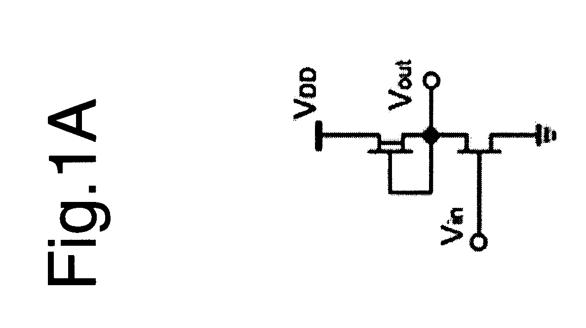
DCFL Ring Oscillator

[0153]FIG. 1B shows a schematic circuit diagram of a DCFL ring oscillator, which is formed with an odd-numbered E / D inverter chain. Seventeen-stage ring oscillators were fabricated with inverters' β=6.7, 10, and 25. For each ring oscillator, 36 transistors were used including an output buffer. FIG. 1D shows a photomicrograph of a fabricated ring oscillator according to the present innovations. The ring oscillators were characterized on-wafer using an Agilent E4404B spectrum analyzer and an HP 54522A oscilloscope. The DC power consumption was also measured during the ring oscillators' operation. FIGS. 44 and 45 show the frequency- and time-domain characteristics of the 17-stage ring oscillator with β=10 biased at VDD=3.5 V. The fundamental oscillation frequency is 225 MHz. According to the formula of propagation delay per stage τpd=(2nƒ)−1, where the number of stages n is 17, and τpd was calculated to be 130 ps / stage. The dependences of τpd and power-delay produc...


PUM


Abstract

Methods and devices for fabricating AlGaN/GaN normally-off high electron mobility transistors (HEMTs). A fluorine-based (electronegative ions-based) plasma treatment or low-energy ion implantation is used to modify the drain-side surface field distribution without the use of a field plate electrode. The off-state breakdown voltage can be improved and current collapse can be completely suppressed in LDD-HEMTs with no significant degradation in gains and cutoff frequencies.

Description

CROSS-REFERENCE TO RELATED APPLICATIONS [0001] This application claims priority from U.S. Provisional Patent Application 60 / 740,256 filed on Nov. 29, 2005, and also from U.S. Provisional Patent Application 60 / 748,339 filed on Dec. 8, 2005, both of which are hereby incorporated by reference.BACKGROUND AND SUMMARY [0002] The present application relates to a method for breakdown voltage enhancement and current collapse suppression in normally-off high electron mobility transistors (“HEMTs”), and in particular, to fabrication of aluminum-gallium nitride / gallium nitride (“AlGaN / GaN”) HEMTs using electrode-less drain-side surface field engineering, resulting in a “Low Density Drain” HEMT. [0003] Excessive electric field can create problems in semiconductor devices. (One type of problem is hot carriers, where sufficiently energetic electrons or holes become able to travel through dielectrics; another type of problem is avalanching, where conduction becomes uncontrolled.) Even in devices de...

Claims


Application Information

Patent Timeline
Patent Type & Authority Applications(United States)
IPC IPC(8): H01L29/778H01L21/338
CPCH01L29/2003H01L29/7786H01L29/66462
Inventor CHEN, JINGLAU, KEL MAY
Owner THE HONG KONG UNIV OF SCI & TECH
Why Eureka
Try Eureka