Semiconductor device and display device including the same

a display device and semiconductor technology, applied in the field of semiconductor circuits and display devices, can solve the problems of increasing the area increasing the manufacturing cost of semiconductor circuits or display devices, etc., and achieve the effect of simplifying the circuit configuration of a/d converter circuits, simplifying the configuration of comparator circuits, and improving the resolution of signal conversion

Inactive Publication Date: 2011-08-18
SEMICON ENERGY LAB CO LTD
View PDF99 Cites 53 Cited by
  • Summary
  • Abstract
  • Description
  • Claims
  • Application Information

AI Technical Summary

Benefits of technology

[0013]According to one embodiment of the present invention, the configuration of a comparator circuit can be simplified, so that the circuit configuration of an A / D converter circuit can be simplified.
[0014]Moreover, according to one embodiment of the present invention, a transistor the threshold voltage of which can be controlled is used in a comparator circuit; thus, it is possible to set the value of a digital signal, which is an output signal of an A / D converter circuit, by setting freely a voltage applied to a second gate of the transistor, so that the resolution of signal conversion can be improved.

Problems solved by technology

However, when an A / D converter circuit has a complicated circuit configuration to have high-performance, the area of the semiconductor circuit or display device increases and the manufacturing cost of a semiconductor circuit or display device may increase.

Method used


Image

  • Semiconductor device and display device including the same
  • Semiconductor device and display device including the same
  • Semiconductor device and display device including the same

Examples


embodiment 1

[0033]In this embodiment, a semiconductor circuit capable of converting an input signal into a digital signal will be described.

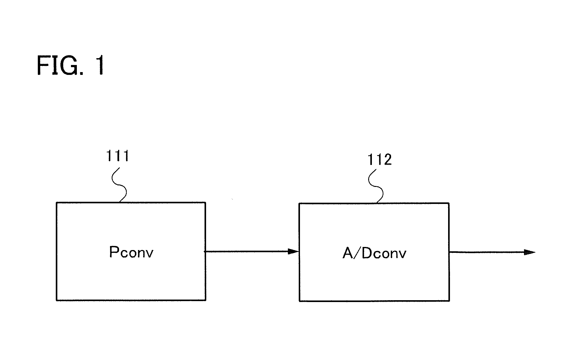
[0034]An example of the configuration of the semiconductor circuit of this embodiment will be described with reference to FIG. 1. FIG. 1 is a block diagram showing an example of the configuration of the semiconductor circuit of this embodiment.

[0035]A semiconductor circuit shown in FIG. 1 includes a photoelectric conversion circuit (also referred to as Pconv) 111 and an A / D converter circuit 112.

[0036]The photoelectric conversion circuit 111 has a function of generating, when receiving light, a voltage V11 the value of which corresponds to the intensity of the light, and outputting the generated voltage V11 as a signal S11. Note that the photoelectric conversion circuit 111 is not necessarily provided. It is only necessary that a voltage with a predetermined wave form is inputted to the A / D converter circuit 112 as an input signal.

[0037]Note that voltage ge...

embodiment 2

[0077]In this embodiment, an example of a photoelectric conversion circuit applicable to the semiconductor circuit in Embodiment 1 will be described.

[0078]An example of the circuit configuration of a photoelectric conversion circuit of this embodiment will be described with reference to FIG. 5. FIG. 5 is a circuit diagram showing an example of the circuit configuration of the photoelectric conversion circuit in FIG. 1.

[0079]A photoelectric conversion circuit shown in FIG. 5 includes a photoelectric conversion element 111a, a transistor 111b, a transistor 111c, and a transistor 111d.

[0080]The photoelectric conversion element 111a has a function of generating, when receiving light, photocurrent in accordance with the intensity of the light. The photoelectric conversion element 111a has a first terminal and a second terminal. A signal S31 is inputted to the first terminal of the photoelectric conversion element 111a. The photoelectric conversion element 111a can be a photodiode or a p...

embodiment 3

[0105]In this embodiment, an example of a display device whose pixel portion employs a photodetection unit will be described.

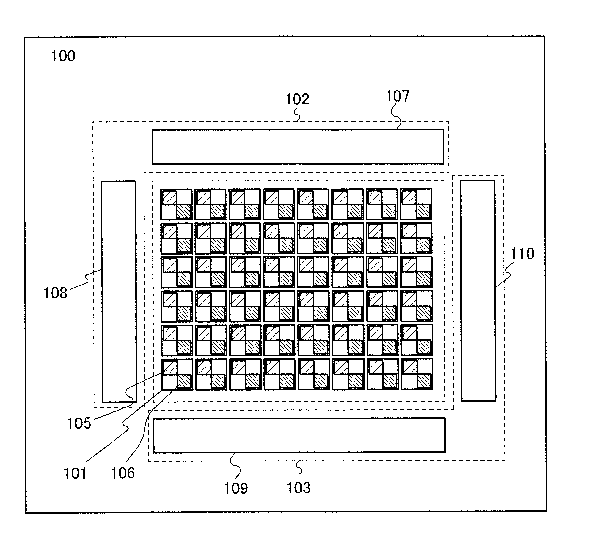
[0106]First, an example of the structure of a display device of this embodiment will be described with reference to FIG. 7. FIG. 7 is a block diagram showing an example of the structure of the display device of this embodiment.

[0107]A display device 100 shown in FIG. 7 includes a pixel portion and a driver circuit area.

[0108]The pixel portion includes a plurality of pixels. The driver circuit area includes driver circuits for controlling the operation of the pixels (e.g., display operation and read (also referred to as readout) operation).

[0109]The pixel portion includes pixel circuits 101. The driver circuit area includes a display circuit controller circuit 102 and a photosensor controller circuit 103.

[0110]Each of the pixel circuits 101 includes a display circuit (also referred to as a display element) 105 and a photosensor 106.

[0111]Next, an example of the...


PUM


Abstract

A semiconductor circuit including: an A/D converter circuit which converts an inputted first signal into a second signal. The A/D converter circuit includes a comparator circuit which compares a voltage of the first signal and a reference voltage; an A/D conversion controller circuit which outputs a digital signal in accordance with comparison results given by the comparator circuit, as a fourth signal and which outputs, in accordance with the third signal, a digital signal corresponding to the first signal, as the second signal; and a D/A converter which converts an inputted fourth signal into an analog signal and which outputs the analog signal as the reference signal. The comparator circuit includes a transistor having a first gate and a second gate. The first signal is inputted to the first gate, the reference signal is inputted to the second gate.

Description

TECHNICAL FIELD[0001]One embodiment of the present invention relates to a semiconductor circuit and a display device.BACKGROUND ART[0002]In recent years, semiconductor devices with light-detecting sensors (also referred to as photosensors, photosensor circuits, or photoelectric conversion circuits) have attracted attention. For example, display devices with photosensors used as touch sensors, are called touch panels, touch screens (also referred to as touch panels), or the like. The touch panel includes photosensors in a display area and thus the display area also functions as an input area. An example of touch panels is display devices with an image capture function (see Patent Document 1, for example). Examples of semiconductor circuits including a photosensor are CCD image sensors and CMOS image sensors. Semiconductor circuits such as CCD image sensors or CMOS image sensors are used, for example, in electronic appliances such as digital still cameras or cellular phones.[0003]In a...

Claims


Application Information

Patent Timeline
Patent Type & Authority Applications(United States)
IPC IPC(8): G06F3/038H03M1/00
CPCG09G3/3648H03M1/46H03K5/2472G09G2360/142H01L27/1251H01L27/1225
Inventor KUROKAWA, YOSHIYUKI
Owner SEMICON ENERGY LAB CO LTD
Why Eureka
Try Eureka