Battery protective device and semiconductor integrated circuit device

a battery protective device and integrated circuit technology, applied in the direction of safety/protection circuits, secondary cells servicing/maintenance, pulse techniques, etc., can solve the problems of overheating the circuit loss of the battery protective device and the semiconductor integrated circuit device according to the invention is low, and the “on” resistance of the battery protective device and the semiconductor integrated circuit device according to the invention is rather high, and the effect of preventing the thermal destruction of the semiconductor devi

Inactive Publication Date: 2008-11-13
FUJI ELECTRIC CO LTD
View PDF5 Cites 59 Cited by
  • Summary
  • Abstract
  • Description
  • Claims
  • Application Information

AI Technical Summary

Benefits of technology

[0027]The “ON” resistance of the battery protective device and the semiconductor integrated circuit device according to the invention is set rather high by controlling a part of the parallel switching elements formed on the semiconductor device. Current is detected by a charge current detector in an overdischarge state, and by a discharge current detector in an overcharge state. To counter the detrimental effect of a parasitic diode, the current is controlled by use of a charge control semiconductor device and a discharge control semiconductor device which are interposed in series with each other in a charge / discharge current path. This makes circuit loss low, prevents thermal destruction of the semiconductor device and makes it easy to detect charge and discharge current as well as the current's direction in a simple circuit configuration.
[0028]The battery protective device provided by the invention can suppress power loss without parasitic diode effects when current is detected through the discharge control semiconductor device and the charge control semiconductor device. Since power loss is suppressed, less heat is generated thus preventing the semiconductor device from thermal destruction. Because a switch-associated parasitic diode is not used, the voltage potential of an impurity diffusion area is not at a diode's forward potential, so extra current is not generated in the substrate and in the power supply.
[0029]A semiconductor integrated circuit device is used to form the charge and discharge control semiconductor devices and the control circuit controlling the semiconductor device's ON and OFF states on the same chip. This operates to suppress malfunction caused by power supply fluctuation and / or latch-up and the like as a result of less current sneaking into the control circuit. Further, since only a part of the parallel switch is made to turn ON, a higher “ON” resistance is obtained. An additional advantage is that the direction of current can be easily detected with high accuracy even in a very low current condition.

Problems solved by technology

Thus, the loss by forward voltage of the parasitic diode Dp2 generates heat, which can overheat the semiconductor integrated circuit (IC) device.
If the discharge occurs with a high current, the semiconductor device can be thermally destructed.
Thus, the same as above, the loss by forward voltage of the parasitic diode Dp1 generates heat and can overheat the semiconductor integrated circuit device.
If the charge occurs with a high current, the semiconductor device can be thermally destructed.
Therefore it is very difficult to detect the direction of current in such a case in order to detect the voltage drop caused by charge / discharge current through charge / discharge FETs because voltage drops through them are very low.
Since the voltage difference between two points (a source and drain of an FET) is measured where neither point is at ground potential, the circuit structure for solving this current detection problem has been difficult.
Thus the parasitic diode is likely to cause extra current to flow in the substrate of an integrated circuit or in a power supply circuit.
Especially in a device with a bi-directional switch and a control circuit that controls the ON and OFF states of the switch that are formed in the same semiconductor substrate, the semiconductor device is likely to malfunction due to power fluctuations and / or latch up caused by current sneaking this way into the circuit part.

Method used


Image

  • Battery protective device and semiconductor integrated circuit device
  • Battery protective device and semiconductor integrated circuit device
  • Battery protective device and semiconductor integrated circuit device

Examples


Embodiment Construction

[0041]A preferred embodiment of the invention will be described with reference to the accompanying drawings.

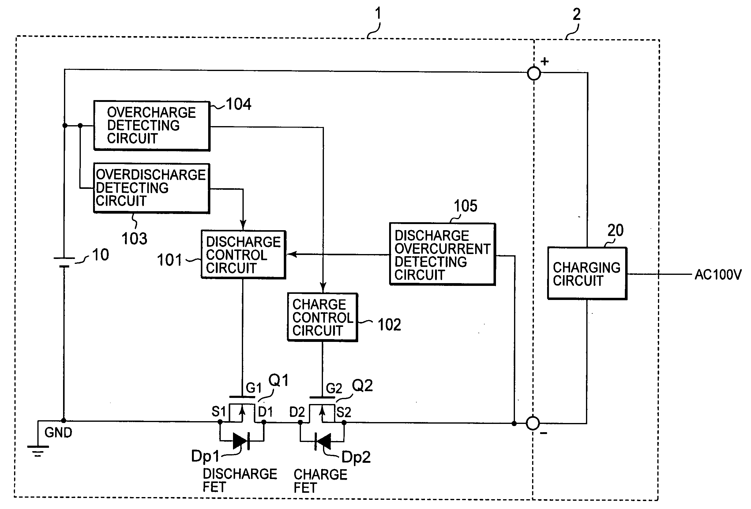
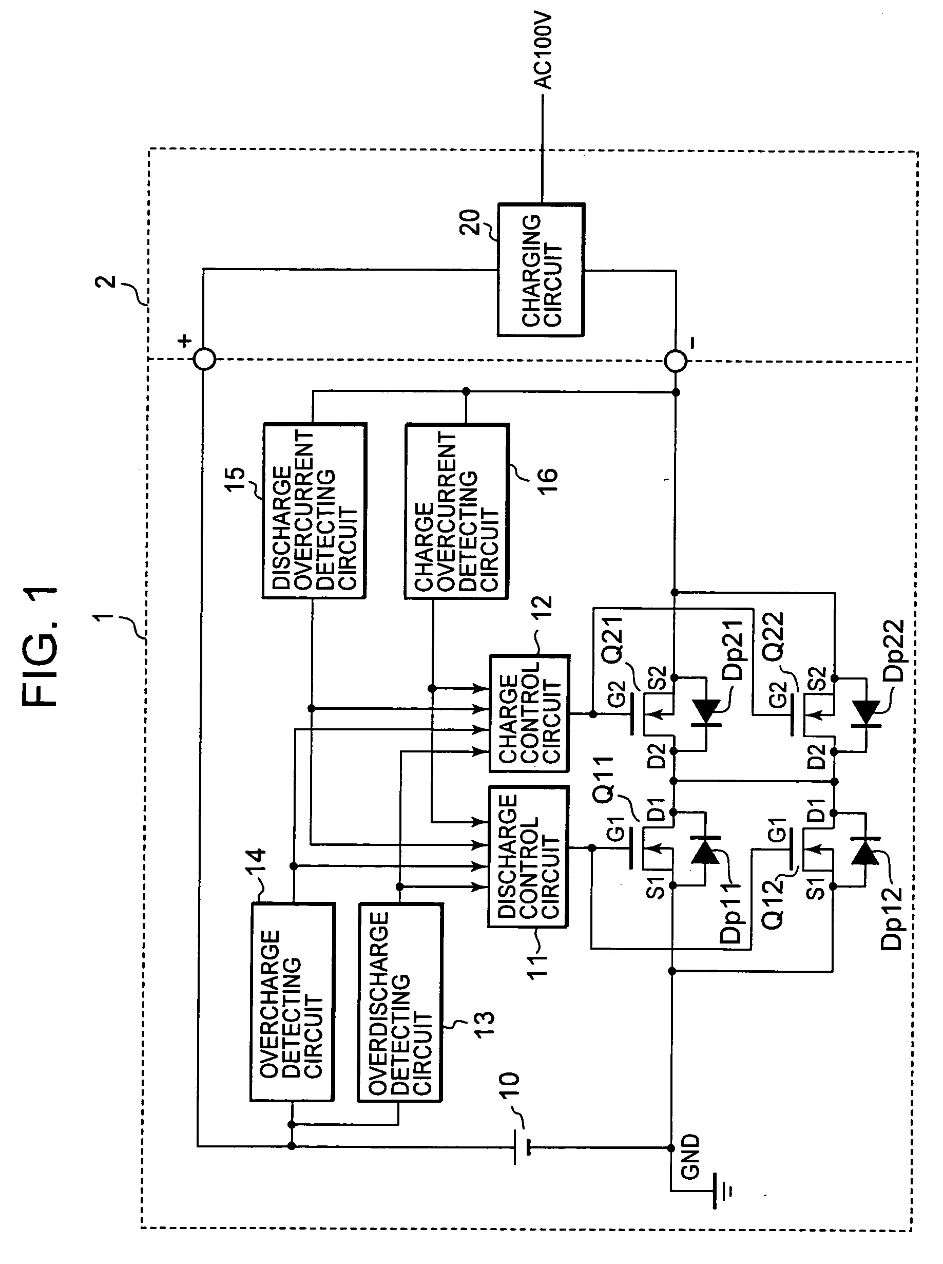
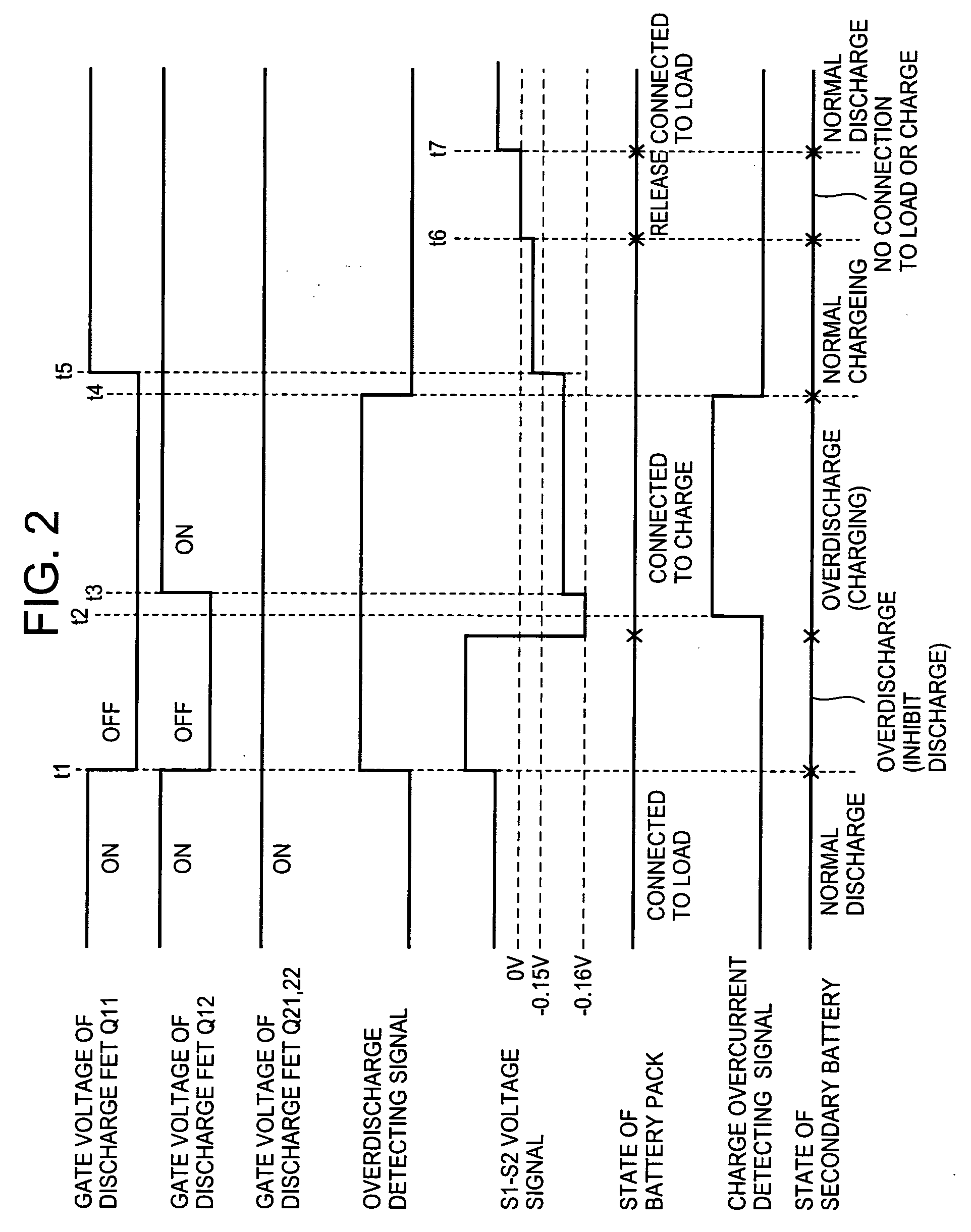
[0042]FIG. 1 is a block diagram showing a circuit structure of the battery protective device relating to a preferred embodiment of the invention. It shows a charger 2 with a charging circuit 20 connected to a battery pack 1. The battery pack 1 includes: a battery 10; discharge FETs Q11 and Q12 for discharge control of semiconductor devices which control the discharge current of the battery 10; charge FETs Q21 and Q22 for charge control of semiconductor devices which control the charge current of the battery 10; discharge control circuit 11, which controls “ON” and “OFF” of the discharge FETs Q11 and Q12; charge control circuit 12 which controls “ON” and “OFF” of the charge FETs Q21 and Q22; an overdischarge detecting circuit 13, which detects overdischarge of the battery 10; an overcharge detecting circuit 14, which detects overcharge of the battery 10; a discharge overcurrent...


PUM


Abstract

A battery protective device that protects against battery damage and semiconductor destruction from overdischarge and overcharge of the battery. Resistance across switching elements is controllable to prevent current leakage through parasitic dipole elements in the integrated circuit. Current is detected with an overdischarge detecting circuit and an overcharge detecting circuit. Direction of the current to/from the battery is detected by discharge overcurrent and charge overcurrent detecting circuits. Switching discharge FETs and charge FETs are enabled as independently controlled, ON-OFF parallel switching elements, interposed in series in the charge/discharge current path of the battery. Only a part of the discharge or charge switching FETs can be turned ON and OFF for accurate current control in accordance with the detected current and its direction.

Description

FIELD OF THE INVENTION[0001]The present invention relates to a battery protective device and to a semiconductor integrated circuit device which protects a battery, such as a lithium ion battery. More particularly, the invention is directed to an apparatus and method for protecting the battery by preventing thermal destruction of a semiconductor device that controls charge and discharge current of the battery.BACKGROUND OF THE INVENTION[0002]A battery pack which holds a battery, such as a lithium ion battery, contains a protective integrated circuit which protects the battery, such as a secondary battery, from overdischarge and overcharge. FIG. 6 is a block diagram which shows a circuit structure of a conventional battery protective device contained in a battery pack, wherein the battery pack 1 is connected to a charger 2.[0003]The battery pack 1 is comprised of a discharge FET Q1, which is a discharge control semiconductor device, a charge FET Q2, which is a charge control semicondu...

Claims


Application Information

Patent Timeline
Patent Type & Authority Applications(United States)
IPC IPC(8): H02J7/00
CPCH01M10/0525H01M10/44H01M10/48H02J7/0031H03K17/6874H02J2007/004H03K17/063H03K17/0822H02J2007/0037H02J7/00306H02J7/00302Y02E60/10H02J7/00304
Inventor MATSUNAGA, SHINICHIRO
Owner FUJI ELECTRIC CO LTD
Why Eureka
Try Eureka