

Surface acoustic wave device, surface acoustic wave apparatus, and communications equipment
A surface acoustic wave and communication device technology, which is applied in the manufacture/assembly of electrical components, piezoelectric/electrostrictive devices, and the selection of device materials, can solve problems such as increased manufacturing costs, inability to fully improve insulation properties, etc. Effects of preventing pyroelectric damage, preventing deterioration of attenuation characteristics or insulation characteristics outside the passband, and expanding the selection range
- Summary
- Abstract
- Description
- Claims
- Application Information
AI Technical Summary
Problems solved by technology
Method used
Image

Examples
no. 1 Embodiment
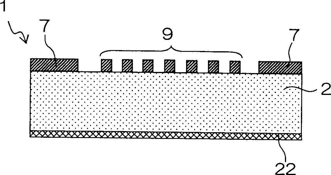
[0214] First, on one main surface of a piezoelectric substrate 2 (substrate thickness: 250 μm) formed by a 38.7° Y-cut X-transport lithium tantalate single crystal substrate, a Ti / Al-1 film was formed from the piezoelectric substrate 2 side by sputtering. 4 conductor layers formed by mass % Cu / Ti / Al-1 mass % Cu. The layer thicknesses are 6nm / 209nm / 6nm / 209nm, respectively.
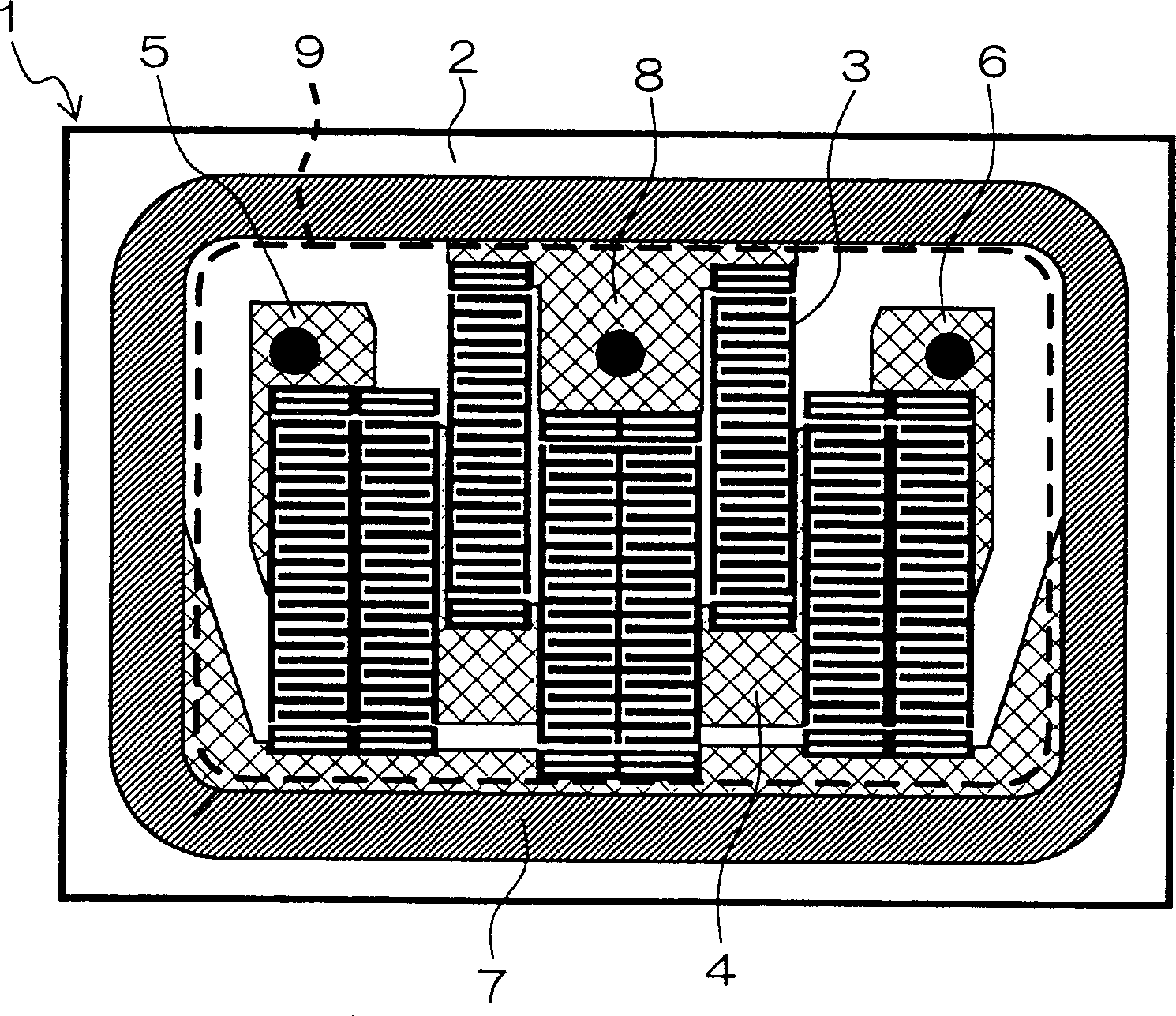
[0215] Next, by photolithography with RIE such as figure 1 This conductive layer is patterned as shown to form a plurality of surface acoustic wave element regions, each of which has a filter region 9 including an IDT electrode 3 , an input electrode portion 5 , and an output electrode portion 6 . The etching gas used at this time is BCl 3 with Cl 2 of mixed gas.
[0216] The electrode finger line width of the comb-shaped electrode forming the IDT electrode 3 and the distance between adjacent electrode fingers are both about 1 μm.
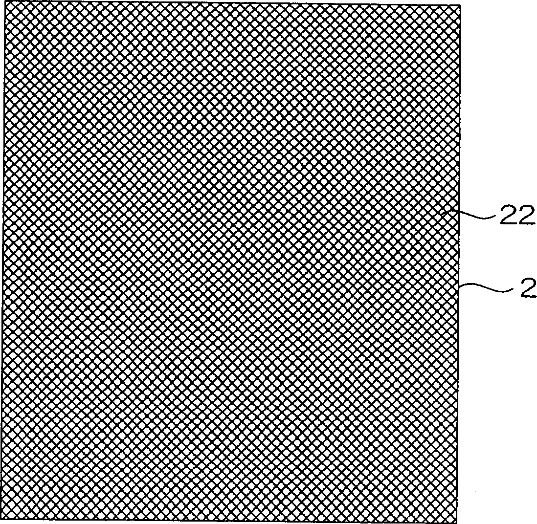
[0217] Next, the semiconductor layer 22 made of silicon to which a tr...
no. 2 Embodiment
[0231] In this embodiment, except that the ring conductor 7 is not provided in the surface acoustic wave element 1, the others are the same as figure 1 Same, but seal construction is different.
[0232] In this example, if Figure 21 As shown in the cross-sectional view, instead of using the annular conductor 7, a sealing structure made of an annular insulator 41 and a covering member 42 for partial protection of the IDT electrode 3 is used to protect the IDT electrode 3, and the surrounding area is covered with an outer coating resin. 34 for protection, providing through-holes reaching from the upper surface of the exterior resin 34 to the input electrode part 5, the output electrode part 6 and the ground electrode part (not shown in the figure), and filling the conductive posts 43 therein as connection electrodes. By adopting such a structure, it is possible to obtain a surface acoustic wave device 40 which is smaller than the case of using the loop conductor 7 .
[0233]...
no. 3 Embodiment
[0239] First, on one main surface of a piezoelectric substrate 2 (substrate thickness: 250 μm) formed by a 38.7° Y-cut X-transport lithium tantalate single crystal substrate, a film of Ti / Al-1 mass is formed from the piezoelectric substrate side by sputtering. 4 conductor layers formed by %Cu / Ti / Al-1 mass % Cu. The film thicknesses are 6nm / 209nm / 6nm / 209nm, respectively.
[0240] Next, by photolithography with RIE such as Figure 4 This conductor layer is patterned as shown to form a plurality of surface acoustic wave device regions, which are respectively formed with the transmission side filter region 12 having the IDT electrode 3, the input electrode portions 5i, 5j, and the output electrode portions 6i, 6j and the reception side filter region 12 and the reception side filter region. device area 13. The etching gas used at this time is BCl 3 with Cl 2 of mixed gas. The line width of the comb-shaped electrodes forming the IDT electrodes 3 and the distance between adjacen...
PUM
| Property | Measurement | Unit |
|---|---|---|
| Thickness | aaaaa | aaaaa |
| Thickness | aaaaa | aaaaa |
| Film thickness | aaaaa | aaaaa |
Abstract
Description
Claims
Application Information