Method of manufacturing semiconductor device and method of manufacturing electronics device

a manufacturing method and semiconductor technology, applied in the direction of semiconductor devices, basic electric elements, electrical equipment, etc., can solve the problems of resin not being disposed of, difficult to fill resin in only a particular position, and evaporation of water contained in the resin filled between the semiconductor packages, so as to avoid separation between the first and second packages and suppress the effect of thermal damage of the resin

Inactive Publication Date: 2007-06-05
SEIKO EPSON CORP
View PDF14 Cites 11 Cited by
  • Summary
  • Abstract
  • Description
  • Claims
  • Application Information

AI Technical Summary

Benefits of technology

[0010]This enables the second semiconductor package to be disposed above the first semiconductor package after the resin is disposed on the first semiconductor package such that the placement position of the resin between the first and second semiconductor packages can easily be adjusted. Thus, even in the case where the gap between the first and second semiconductor packages is narrow, the resin can be disposed between the first and second semiconductor packages avoiding a solder material, while the resin can be provided between the first and second semiconductor packages with ensuring channels for letting out water contained in the resin. As a result, the separation between the first and second semiconductor packages can be avoided while thermal damage of the resin is suppressed. In addition, the first and second semiconductor packages can be secured to each other with the resin, enabling the displacement between the first and second semiconductor packages to be avoided even in the case where a reflow process is implemented during a second mounting.
[0027]Furthermore, even in the case where the resin is disposed on the first package before the second package is disposed above the first package, the fluidity of the resin provided between the first and second packages can be maintained when the second package is electrically coupled to the first package. Thus, even in the case where a solder material is used for electrically coupling the second package to the first package, self-alignment by the surface tension of solder when melted can be utilized, enabling the second package to be precisely disposed above the first package.

Problems solved by technology

Thus, when the resin filled between the semiconductor packages is cured, water contained in the resin is not sufficiently removed such that some water remains in the resin filled between the semiconductor packages.
This causes a problem that, when a reflow process is implemented during a secondary mounting of the stacked semiconductor packages, water contained in the resin filled between the semiconductor packages evaporates and expands such that the separation between the semiconductor packages occurs.
It is therefore difficult to fill resin into only a particular position between semiconductor packages if the gap between the semiconductor packages is narrow.
This causes problems that the resin gets in contact with solder balls so as to cause thermal damage to the resin and the resin can not be disposed in consideration of stress applied to the semiconductor packages.
Meanwhile, if semiconductor packages are secured to each other with resin before the semiconductor packages are fixed to each other through the solder balls, the semiconductor packages get stuck when the solder balls are reflowed.
As a result, there has been a problem that self-alignment of the semiconductor packages by the surface tension of the solder balls when melted is prevented such that the placement accuracy of the semiconductor packages is degraded.

Method used


Image

  • Method of manufacturing semiconductor device and method of manufacturing electronics device
  • Method of manufacturing semiconductor device and method of manufacturing electronics device
  • Method of manufacturing semiconductor device and method of manufacturing electronics device

Examples


first embodiment

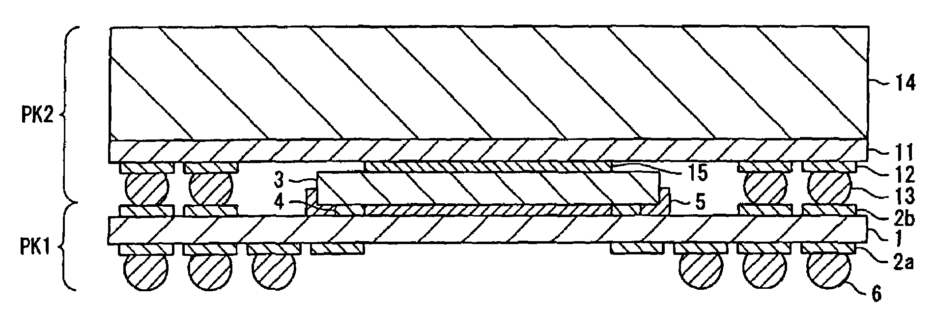
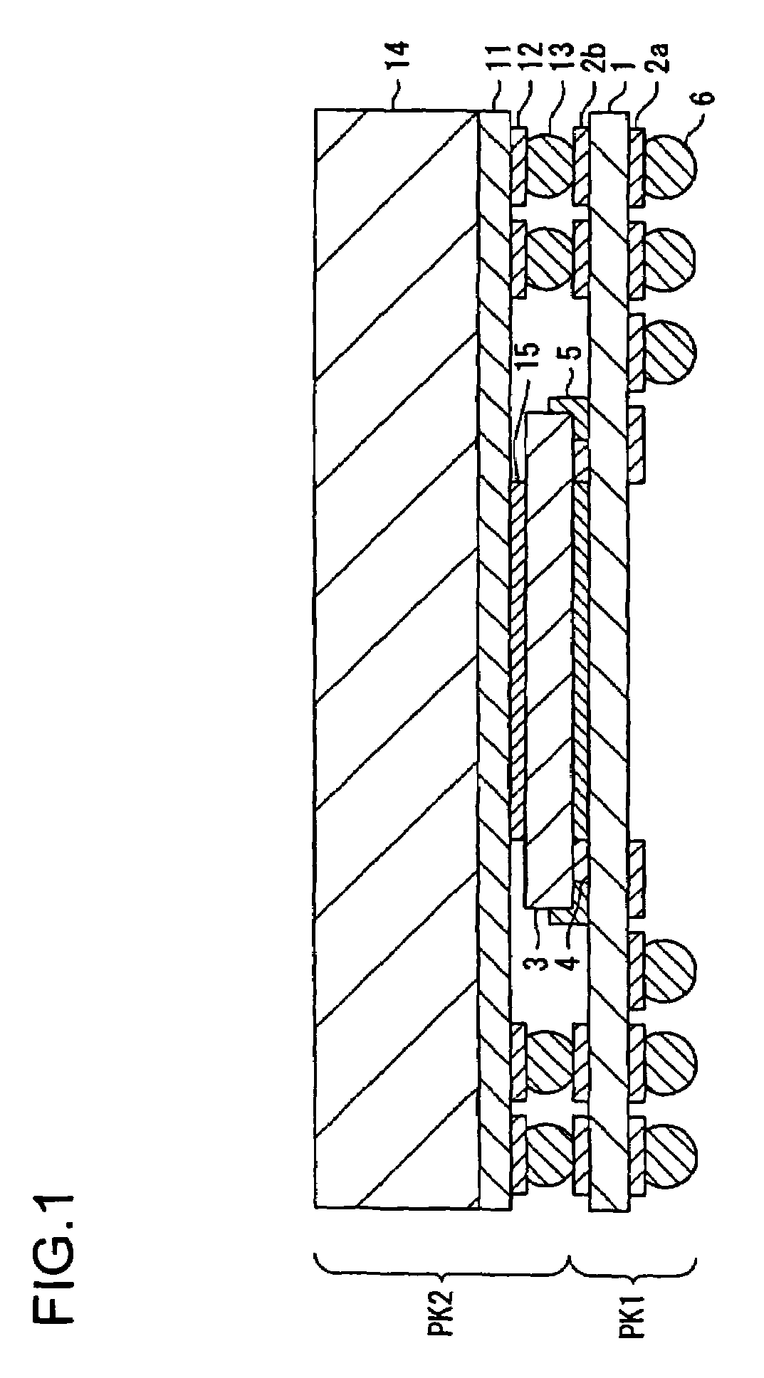
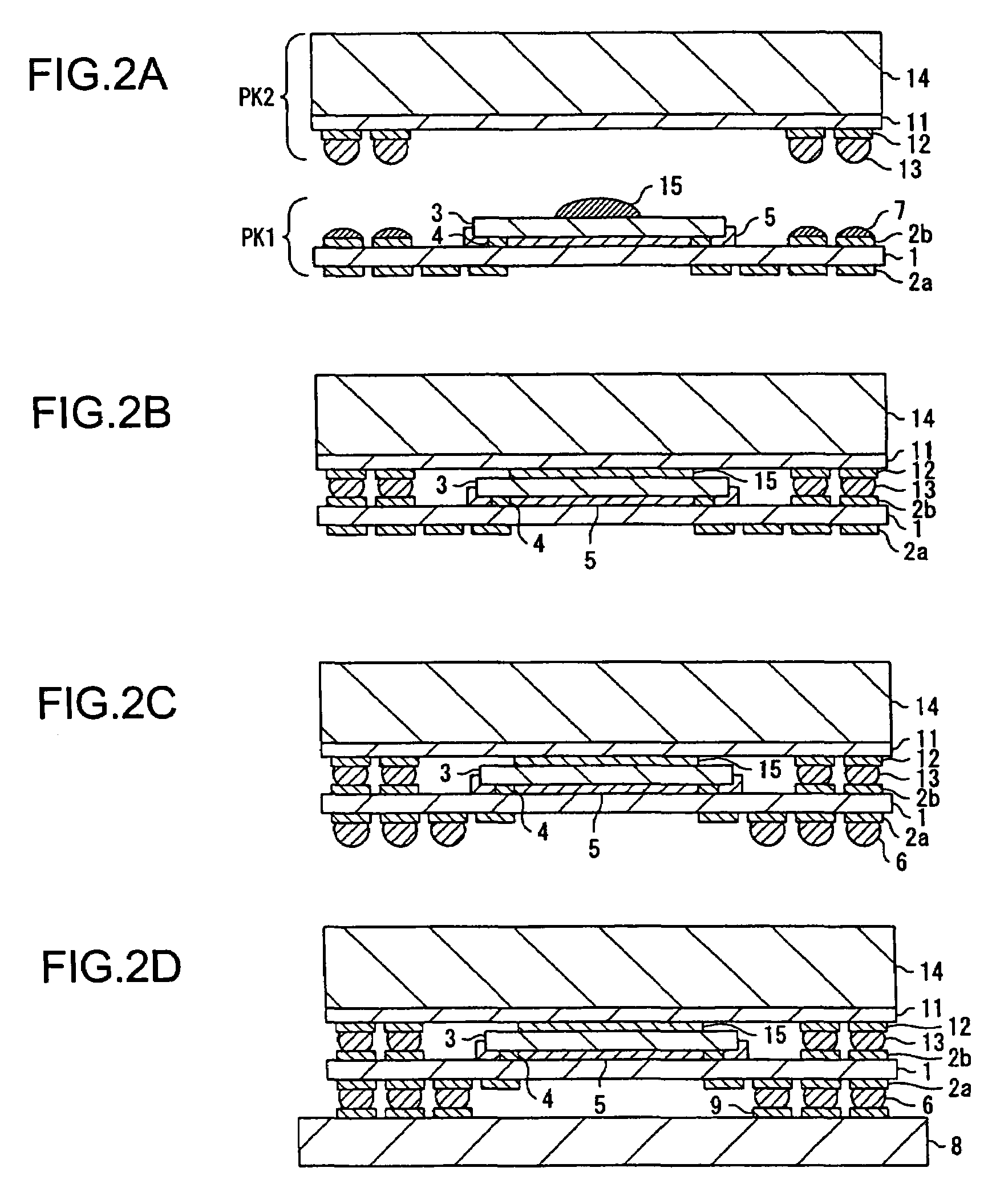
[0035]FIG. 1 is a sectional view schematically showing a structure of a semiconductor device according to the present invention.

[0036]Referring to FIG. 1, a semiconductor package PK1 includes a carrier substrate 1, and on both sides of the carrier substrate 1 are formed lands 2a and 2b, respectively. A semiconductor chip 3 is flip-chip mounted on the carrier substrate 1. Protruding electrodes 4 for flip-chip mounting are provided on the semiconductor chip 3. The protruding electrodes 4 provided on the semiconductor chip 3 are bonded to the lands 2b through an anisotropic conductive sheet 5 by Anisotropic Conductive Film (ACF) bonding.

[0037]Meanwhile, a semiconductor package PK2 includes a carrier substrate 11. Lands 12 are formed on a back surface of the carrier substrate 11, and protruding electrodes 13 are provided on the lands 12. A semiconductor chip is mounted on the carrier substrate 11. The carrier substrate 11, where the semiconductor chip is mounted, is sealed with a sealin...

second embodiment

[0059]FIG. 3 is a sectional view schematically showing a structure of a semiconductor device according to the present invention.

[0060]Referring to FIG. 3, a semiconductor package PK11 includes a carrier substrate 21. Lands 22a and 22c are formed on both sides of the carrier substrate 21, respectively, and an internal wiring 22b is formed inside the carrier substrate 21. A semiconductor chip 23 is flip-chip mounted on the carrier substrate 21. Protruding electrodes 24 for flip-chip mounting are provided on the semiconductor chip 23. The protruding electrodes 24 provided on the semiconductor chip 23 are bonded to the lands 22c through an anisotropic conductive sheet 25 by ACF bonding. On the lands 22a provided on a back surface of the carrier substrate 21, provided are protruding electrodes 26 for mounting the carrier substrate 21 on a motherboard.

[0061]Meanwhile, a semiconductor package PK12 includes a carrier substrate 31. Lands 32a and 32c are formed on both sides of the carrier su...

third embodiment

[0066]FIG. 4 is a sectional view schematically showing a structure of a semiconductor device according to the present invention.

[0067]Referring to FIG. 4, a semiconductor package PK21 includes a carrier substrate 41. Lands 42a and 42c are formed on both sides of the carrier substrate 41, respectively, and an internal wiring 42b is formed inside the carrier substrate 41. A semiconductor chip 43 is flip-chip mounted on the carrier substrate 41. Protruding electrodes 44 for flip-chip mounting are provided on the semiconductor chip 43. The protruding electrodes 44 provided on the semiconductor chip 43 are bonded to the lands 42c through an anisotropic conductive sheet 45 by ACF bonding. On the lands 42a provided on a back surface of the carrier substrate 41, provided are protruding electrodes 46 for mounting the carrier substrate 41 on a motherboard.

[0068]Meanwhile, a semiconductor package PK22 includes a carrier substrate 51. To the semiconductor chip 51, provided are electrode pads 52...


PUM


Abstract

A method of manufacturing a semiconductor device includes providing resin on at least a partial area on a first semiconductor package and coupling a second semiconductor package to the first semiconductor package electrically while the resin maintains its fluidity.

Description

BACKGROUND OF THE INVENTION[0001]1. Field of the Invention[0002]The present invention relates to a method of manufacturing a semiconductor device and a method of manufacturing an electronic device, and especially relates to methods that are preferably applied to a stack structure of semiconductor packages.[0003]2. Description of the Related Art[0004]In a conventional semiconductor package, space-saving has been attempted by stacking semiconductor packages through solder balls. In this method, resin is filled between the stacked semiconductor packages.[0005]In a conventional semiconductor package, however, resin is filled into the entire gap between semiconductor packages stacked through solder balls. Thus, when the resin filled between the semiconductor packages is cured, water contained in the resin is not sufficiently removed such that some water remains in the resin filled between the semiconductor packages. This causes a problem that, when a reflow process is implemented during ...

Claims


Application Information

Patent Timeline
Patent Type & Authority Patents(United States)
IPC IPC(8): H01L21/00H01L21/98H01L25/10
CPCH01L25/105H01L25/50H01L2224/16H01L2224/32145H01L2224/32225H01L2224/48095H01L2224/48227H01L2224/48465H01L2224/73265H01L2924/01079H01L2924/15311H01L2224/73204H01L2224/16225H01L2924/00H01L2224/73253H01L2924/15331H01L2924/00012H01L2225/1023H01L2225/1058H01L2225/1005H01L2924/181H01L24/73
Inventor AOYAGI, AKIYOSHI
Owner SEIKO EPSON CORP
Why Eureka
Try Eureka