Display device and method for adjusting a voltage for driving a display device

a display device and voltage technology, applied in the field of display devices, can solve the problems of increasing the cost of parts as a large number of photodiodes are used, and achieve the effects of simple circuit configuration, increased flicker detection points, and low cos

Active Publication Date: 2007-03-22
PANASONIC LIQUID CRYSTAL DISPLAY CO LTD +1
View PDF4 Cites 51 Cited by
  • Summary
  • Abstract
  • Description
  • Claims
  • Application Information

AI Technical Summary

Benefits of technology

[0016] In a display device having a function of automatically adjusting a common electrode voltage VCOM, flicker detection points can be increased in an inexpensive and simple circuit configuration. By increasing the flicker detection points, the VCOM voltage can be automatically adjusted with higher accuracy, and natural images can be displayed without prominent flicker.

Problems solved by technology

Therefore, if a photodiode is provided only at a single point on the display plane for detecting the flicker, this detection strategy can reflect the local flicker at that point but fails to reflect flicker which can occur on the display plane other than the measuring point at which the photodiode is provided.
When a plurality of photodiodes are provided for detecting the flicker, the part cost increases as a larger number of photodiodes are used.

Method used


Image

  • Display device and method for adjusting a voltage for driving a display device
  • Display device and method for adjusting a voltage for driving a display device
  • Display device and method for adjusting a voltage for driving a display device

Examples


first embodiment

[0027] A first embodiment will be described.

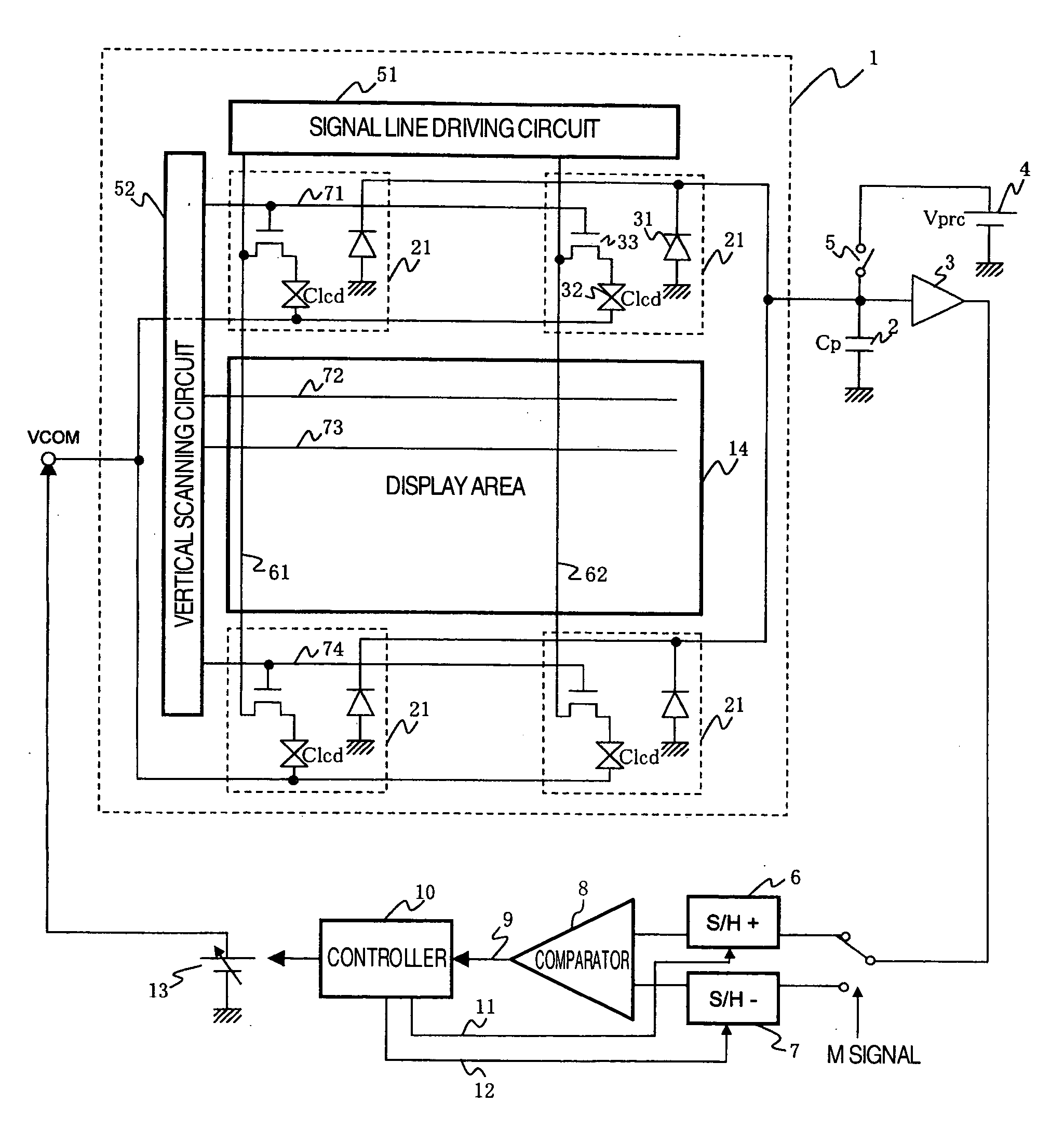
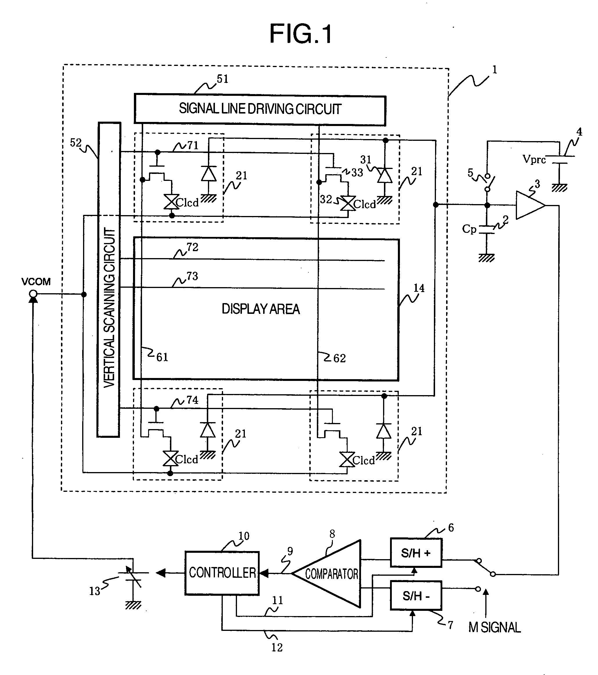
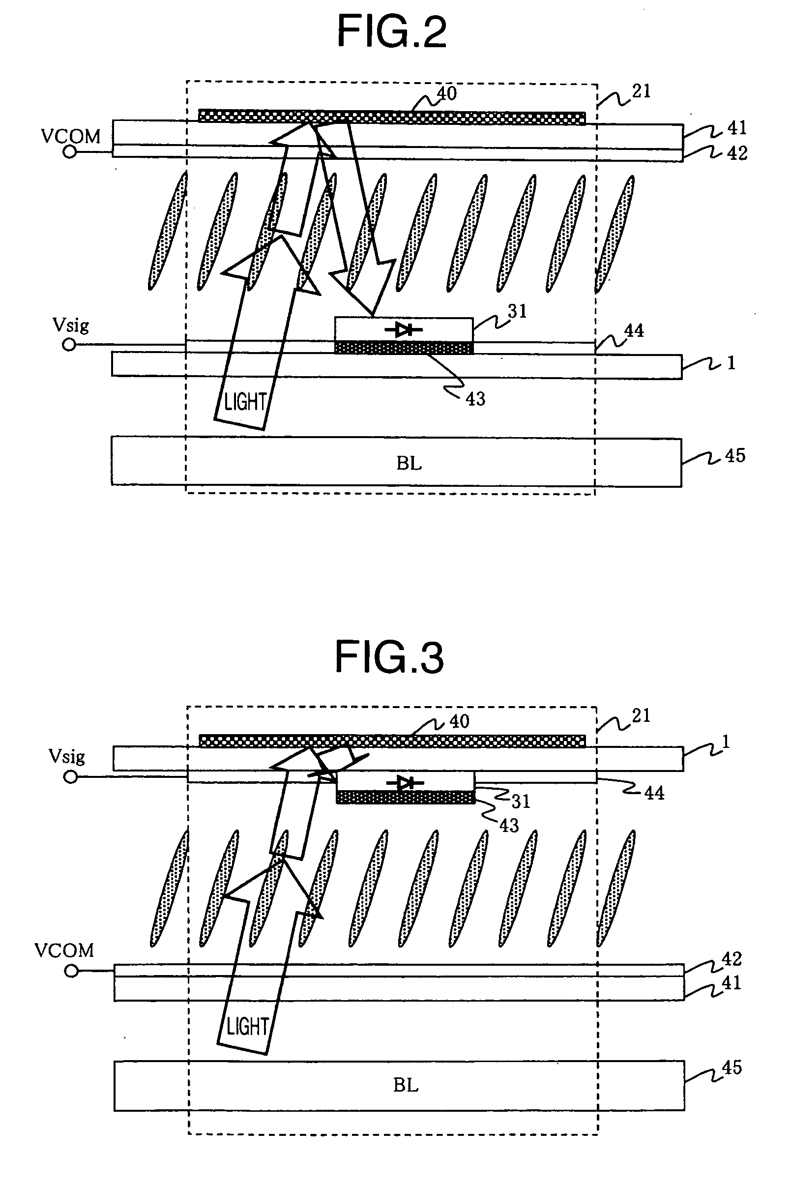
[0028]FIG. 1 is a schematic diagram illustrating an exemplary configuration of a display device having a function of automatically adjusting a common electrode voltage according to the present invention. The display device comprises a TFT array substrate 1; a precharge capacitance (Cp) 2; an analog buffer amplifier 3; a precharge voltage source (Vprc) 4; a precharge switch 5; a sample / hold circuit 6 for use when a positive signal is applied; a sample / hold circuit 7 for use when a negative signal is applied; a comparator 8 which outputs a comparison result 9; a controller 10; a sampling signal 11 for use when the positive signal is applied; a sampling signal 12 for use when the negative signal is applied; a common electrode power supply 13; a display area 14; dummy pixels 21; photodiodes 31; a liquid crystal element (Clcd) 32; TFT elements 33; a signal line driving circuit 51; a vertical scanning circuit 52; a first signal line 61; a secon...

second embodiment

[0059] A second embodiment will be next described.

[0060]FIG. 8 illustrates an exemplary layout of dummy pixels 21. While the dummy pixels 12 are positioned at four corners of the display area 14 in the first embodiment, two or more dummy pixels may be disposed along one horizontal line or along a plurality of horizontal lines, as illustrated in FIG. 8. By thus increasing the number of dummy pixels 21, variations in the characteristics of each output of the signal line driving circuit 51, and variations in the strength of flicker due to the blunted scanning signal waveform shown in FIG. 5 can be more correctly reflected to the adjustment of VCOM.

[0061] While additional dummy pixels 21 are arranged in the horizontal direction in FIG. 8, they may be arranged in the vertical direction. Also, a switch may be provided between the photodiode 31 and the precharge capacitance 2 within the dummy pixel 1, such that when a partial display is performed, the flicker strength can be measured by ...

third embodiment

[0062] A third embodiment will be next described.

[0063]FIG. 9 illustrates an exemplary layout of photodiodes 31 in accordance with the importance of luminance measurement points. When the flicker is to be suppressed preferentially in a central region of the display area 14 rather than left and right marginal regions of the display area 14, a plurality of photodiodes 31 are created in those dummy pixels 21 positioned in the central region to perform a photoelectric conversion in such a manner that more currents flow into the dummy pixels positioned in the central region, thus weighting the dummy pixels 21 according to the measuring points. In other words, a photoelectric conversion rate in the central region of the display area 14 is made different from that in the left and right marginal regions, thus permitting the dummy pixels in the central region, which supply more currents, to more contribute to the discharge of the precharge capacitance 2 and therefore largely affect the disc...


PUM


Abstract

A display device includes a display panel having pixels arranged in a matrix form, a driving circuit for outputting an analog voltage according to a video signal to the pixels through signal lines, a plurality of measuring circuits each for detecting the amount of transmitted light, a single totalizing circuit for totalizing the results of measurements made by the measuring circuits, and a control circuit for adjusting a potential on a common electrode of the display panel in accordance with the result of the totalization from the totalizing circuit. The results of measurements made by the plurality of measuring circuits are totalized by the single totalizing circuit.

Description

CLAIM OF PRIORITY [0001] The present application claims priority from Japanese patent application serial No. 2005-271798 filed on Sep. 20, 2005, the content of which is hereby incorporated by reference into this application. BACKGROUND OF THE INVENTION [0002] The present invention relates to a display device for displaying an image on a display panel illuminated by a back light source, and more particularly, to a display device which can adjust a voltage applied to a common electrode. [0003] In a liquid crystal element used for a display device, a continuously applied DC voltage results in a degradation in image quality similar to burn-in. For this reason, in a liquid crystal display, a liquid crystal element is applied with signal voltages which include a positive voltage (Vsig+) and a negative voltage (Vsig−) alternately applied in each frame period. Also, when a voltage (VCOM) is applied to a common electrode of the liquid crystal element, the display luminance is determined in a...

Claims


Application Information

Patent Timeline
Patent Type & Authority Applications(United States)
IPC IPC(8): G09G3/36
CPCG02F1/13318G09G3/3614G09G3/3655G09G2360/145G09G2320/0247G09G2320/029G09G2320/0223
Inventor AWAKURA, HIROKIKUDO, YASUYUKIMAMBA, NORIO
Owner PANASONIC LIQUID CRYSTAL DISPLAY CO LTD
Why Eureka
Try Eureka