Class D amplifier

a class d amplifier and amplifier technology, applied in the direction of amplifiers, dc amplifiers with modulators/demodulators, semiconductor devices/discharge tubes, etc., can solve the problems of loss of inherent advantages of class d amplifiers, difficulty in turning on one of the switching devices connected to the constant voltage power supply, and increase the consumption power of constant voltage power supplies. , to achieve the effect of reducing distortion in audio signals, simple circuit configuration and high accuracy

Inactive Publication Date: 2005-08-02
MITSUBISHI ELECTRIC CORP
View PDF9 Cites 57 Cited by
  • Summary
  • Abstract
  • Description
  • Claims
  • Application Information

AI Technical Summary

Benefits of technology

[0036]An object of the present invention is to provide a class D amplifier having a simple circuit configuration, capable of reducing distortion in an audio signal with high accuracy, that is, a class D amplifier of high efficiency in which distortion in an output signal due to fluctuations in supply voltage supplied to a power switch is greatly reduced as compared to a conventional amplifier and which can be used without any problem even when the supply voltage varies in a relatively wide range.

Problems solved by technology

However, the above-described method actually causes a problem in that the use of an ideal constant-voltage power supply for the power supply of the power switch is generally difficult to realize on cost grounds and a problem in that consumption power in the constant-voltage power supply is increased, which results in loss of inherent advantages of the class D amplifier.
In view of these problems, compromises have been made in many cases, though not sufficient, which only suppresses an alternating component of audio frequency which particularly comes into question because of an LC filter.
Further, according to the above-described method, the power switching devices forming the power switch each have a finite delay time for turn-on and turn-off.
Therefore, it is generally difficult to turn ON one of the switching device connected to the constant voltage power supply and the switching device connected to the ground, and turn OFF the other one with the same timing.
The above-mentioned fluctuations in the supply voltage directly appear as fluctuations in the amplitude of an output signal from the power switch, causing distortion in an audio signal output from the amplifier.
Further, distortion in an output signal from the power switch resulting from the dead time setting also causes distortion in an audio signal output from the amplifier.
First, in order to improve the effects of correction, the signal Vi input to the “−” terminal of the comparator 202 needs to be converted to a trapezoidal waveform signal of high accuracy. However, generating a trapezoidal waveform signal with high accuracy disadvantageously requires a circuit configuration to be complicated as compared to the circuit shown in FIG.
Second, a pulse modulated signal Vr and feedback signal Vs input to the error handler 101 are pulse signals. It is very difficult to normally generate an error signal Ve from such pulse signals, and remaining pulses in the error signal Ve cannot be removed completely. Such remaining pulses disadvantageously result in difficulty of obtaining sufficient effects of correction.
Actually, however, phase rotation of the feedback signal Vs in the error handler 101 unstabilizes loop operations, which makes it difficult to filter the error handler 101 such that a pulse component is sufficiently attenuated.
On the aforementioned grounds, it is difficult to obtain sufficient effects of correction (reduction of distortion in an audio signal) because of remaining pulses.
However, fluctuations in supply voltage supplied to the power switch disadvantageously cause distortion in an output signal.
If a voltage of a certain value is always supplied to the power switch through a constant voltage circuit, distortion in an output signal may be reduced, however, the power switch consumes relatively great power, and power loss in the constant voltage circuit for supplying a voltage of a certain value to the power switch thus increases, which causes another problem in that power amplification cannot be performed on an audio signal with high efficiency and low power loss.

Method used


Image

  • Class D amplifier
  • Class D amplifier
  • Class D amplifier

Examples


first preferred embodiment

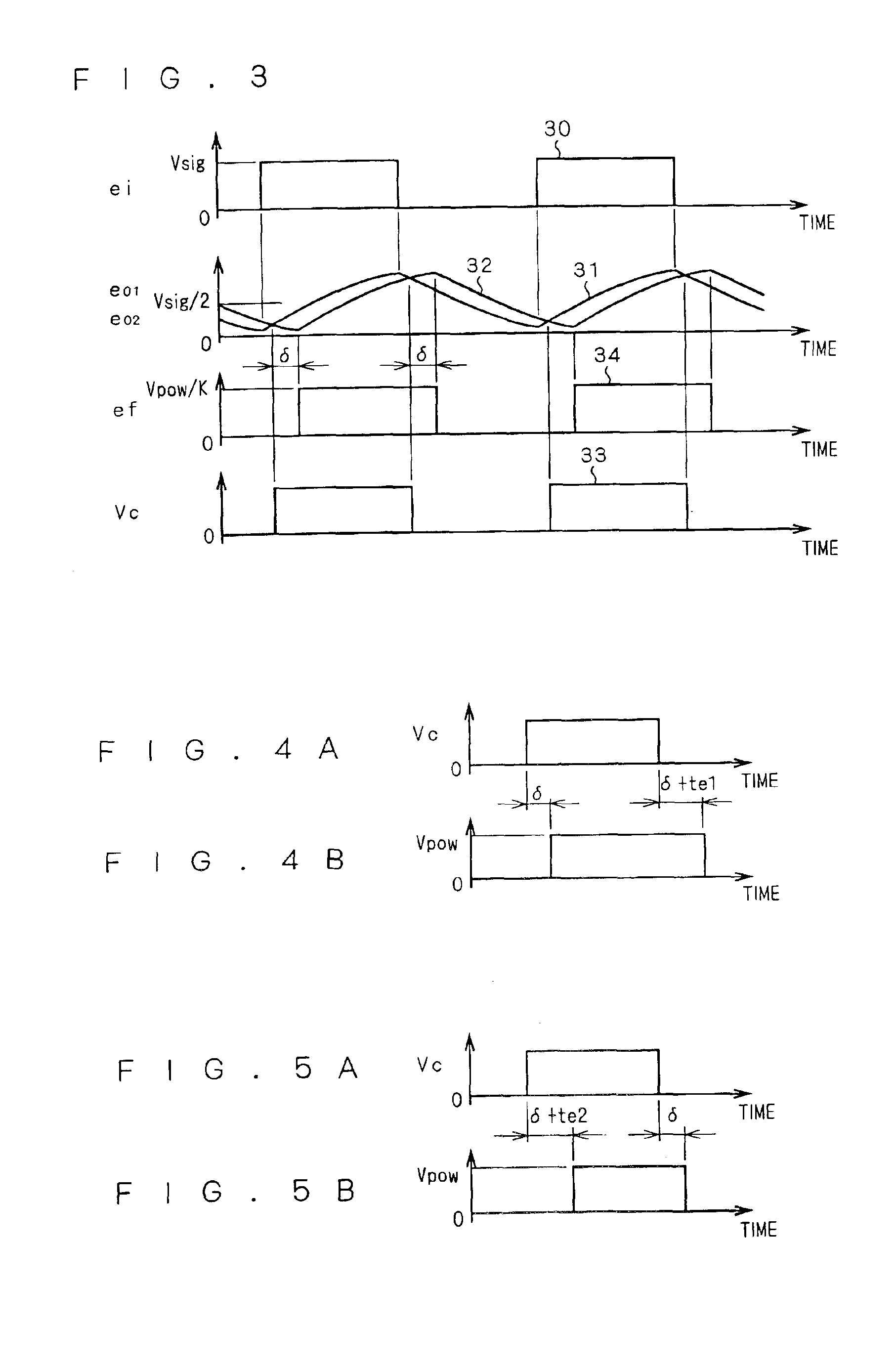
[0084]A correction circuit included in a class D amplifier according to the present embodiment is capable of integrating a pulse modulated signal output from a pulse modulator and a feedback signal output from a power switch, comparing integrated signals in a comparator using the pulse modulated signal as a reference for outputting an output signal corresponding to the result of comparison to the power switch, and finally correcting signal distortion occurring in the power switch.

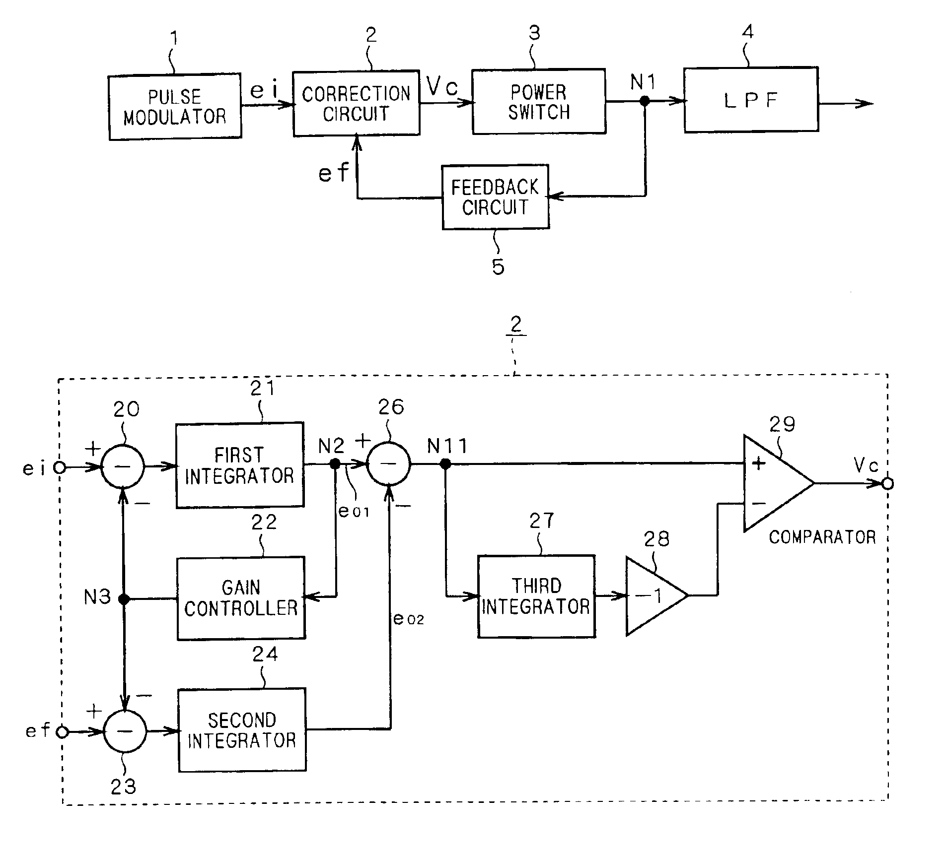
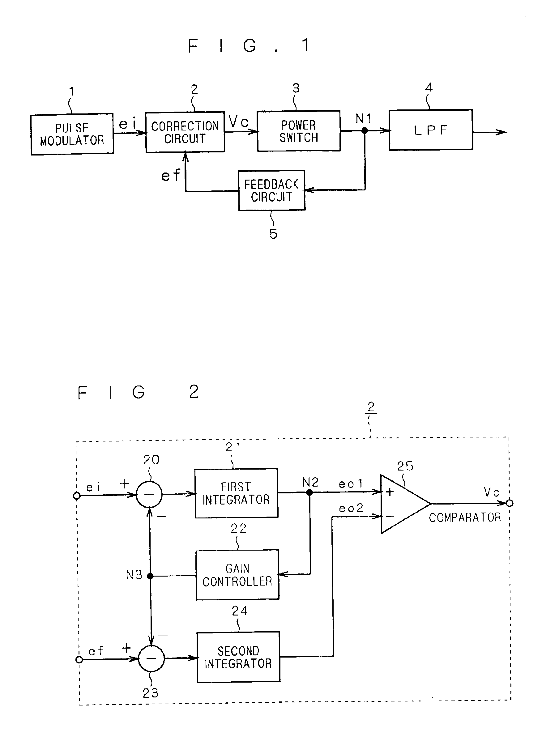
[0085]FIG. 1 is a block diagram illustrating the circuit configuration of the class D amplifier according to the present invention including the correction circuit.

[0086]The class D amplifier illustrated in FIG. 1 includes a pulse modulator 1, a correction circuit 2, a power switch 3 and a low-pass filter (LPF) 4 connected in series to each other. A signal is transmitted from the pulse modulator 1 to the LPF 4. A feedback circuit 5 is provided between a node N1 and the correction circuit 2 such that part of...

second preferred embodiment

[0208]The correction circuit according to the present embodiment is to be incorporated in the class D amplifier shown in FIG. 1 described in the first preferred embodiment. The correction circuit is not for directly comparing a signal from the first integrator and that from the second integrator, but for obtaining the difference between the signal from the first integrator and that from the second integrator in a subtracter and then comparing an output signal (differential signal) from the subtracter and a signal obtained by integrating the differential signal in a third integrator and then reversed in a reverser, thereby generating a correction signal.

[0209]A block diagram of the inner configuration of the correction circuit 2 according to the present embodiment is illustrated in FIG. 13. The configuration shown in FIG. 13 will be specifically described hereinbelow. In FIG. 13, the subtracter 20, first integrator 21, gain controller 22, subtracter 23 and second integrator 24 have t...

third preferred embodiment

[0308]FIG. 22 is a block diagram of the configuration of a class D amplifier according to a third preferred embodiment of the present invention. The class D amplifier comprises the pulse modulator 1, correction circuit 2, power switch 3, LPF 4, feedback circuit 5, a speaker 406, a first constant voltage control circuit 407, a second constant voltage control circuit 408, dc output reference signal generator 410 and an arithmetic unit 411. The class D amplifier is supplied with a supply voltage Vcc from an external source through a power terminal 409.

[0309]The pulse modulator 1 generates a pulse modulated signal, and the power switch 3 performs switching between the power supply and ground in accordance with a correction signal corrected in the correction circuit 2, enabling power supply to a load (speaker 406) connected to the output of the class D amplifier. The switching operation is carried out by switching devices configured as described in the first preferred embodiment.

[0310]Th...


PUM


Abstract

A pulse modulated signal (ei) output from a pulse modulator (1) and a feedback signal (ef) containing distortion caused by a power switch (3) are integrated in a first integrator (21) and a second integrator (24), respectively, and are input to input terminals of a comparator (25 or 29), respectively, so that a correction signal (Vc) is generated.

Description

[0001]This Nonprovisional application claims priority under 35 U.S.C. § 119(a) on Patent Application No(s). 2002-299195, 2002-333412 and 2003-052385 filed in Japan on Oct. 3, 2002, Nov. 18, 2002 and Feb. 28, 2003, respectively, the entire contents of which are hereby incorporated by reference.BACKGROUND OF THE INVENTION[0002]1. Field of the Invention[0003]The present invention relates to a class D amplifier, and more particularly to a class D amplifier having a correction circuit.[0004]2. Description of the Background Art[0005]Class D amplification has conventionally been adopted as a method of enabling device miniaturization by performing power amplification on audio signals with high efficiency and low power loss. A class D amplifier is known in which a digitized audio signal is directly converted to a pulse width modulated signal and is guided to a power switch. The power switch usually includes a switching device connected to a constant voltage power supply and a switching devic...

Claims


Application Information

Patent Timeline
Patent Type & Authority Patents(United States)
IPC IPC(8): H03F3/217H03F3/20H03F99/00
CPCH03F3/217H03F2200/331
Inventor TAURA, KENICHITSUJI, MASAYUKIISHIDA, MASAYUKINAKADA, TSUYOSHI
Owner MITSUBISHI ELECTRIC CORP
Why Eureka
Try Eureka