

Semiconductor device and power conversion device using the same
a technology of semiconductor devices and power conversion devices, applied in semiconductor devices, diodes, electrical apparatus, etc., can solve the problems of large switching loss of igbt, inability to meet the demands of miniaturization, and increased cost of power conversion devices, so as to increase power loss, large switching loss, and increase power loss
- Summary
- Abstract
- Description
- Claims
- Application Information
AI Technical Summary
Benefits of technology
Problems solved by technology
Method used
Image

Examples
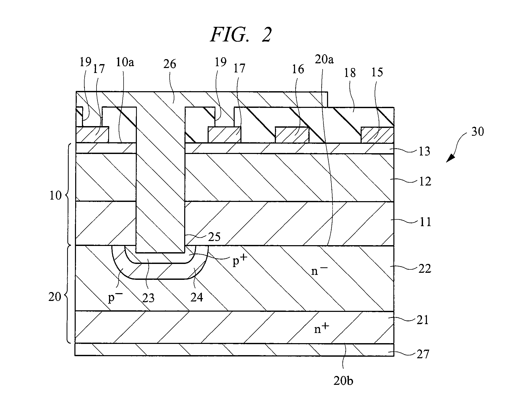
first embodiment
[0038]In a first embodiment, an embodiment in which a semiconductor device provided with a high electron mobility transistor is applied as a switching element of a power conversion device will be described.
[0039]
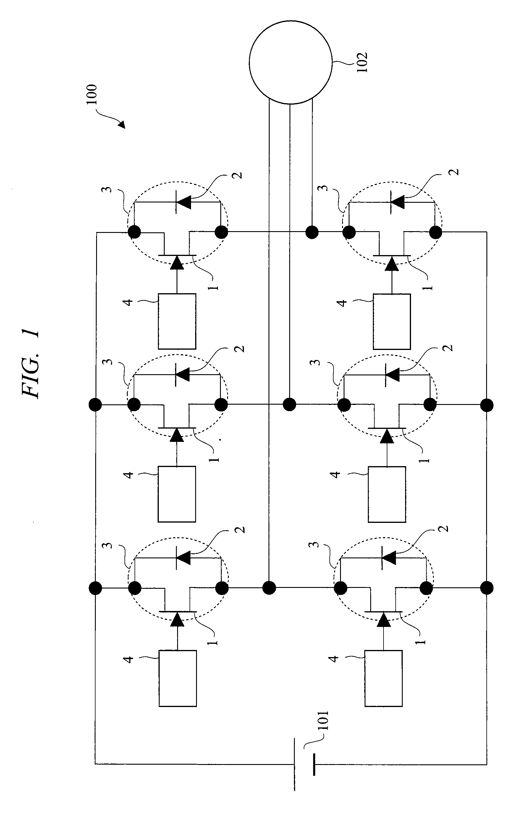
[0040]First, a circuit configuration of the power conversion device of the first embodiment will be described with reference to FIG. 1. FIG. 1 is a circuit diagram of the power conversion device of the first embodiment.
[0041]In FIG. 1, the power conversion device 100 of the first embodiment is, for example, a DC (Direct Current)-AC (Alternating Current) inverter which converts the DC power supplied from a DC power source 101 to three-phase AC power and supplies it to a motor 102 which operates as a load.
[0042]Also, the power conversion method of the power conversion device 100 is a switching method, and a switching element 3 has a transistor 1 and a diode 2. The transistor 1 and the diode 2 are connected in parallel. FIG. 1 shows an example in which a total of six switching ...
second embodiment
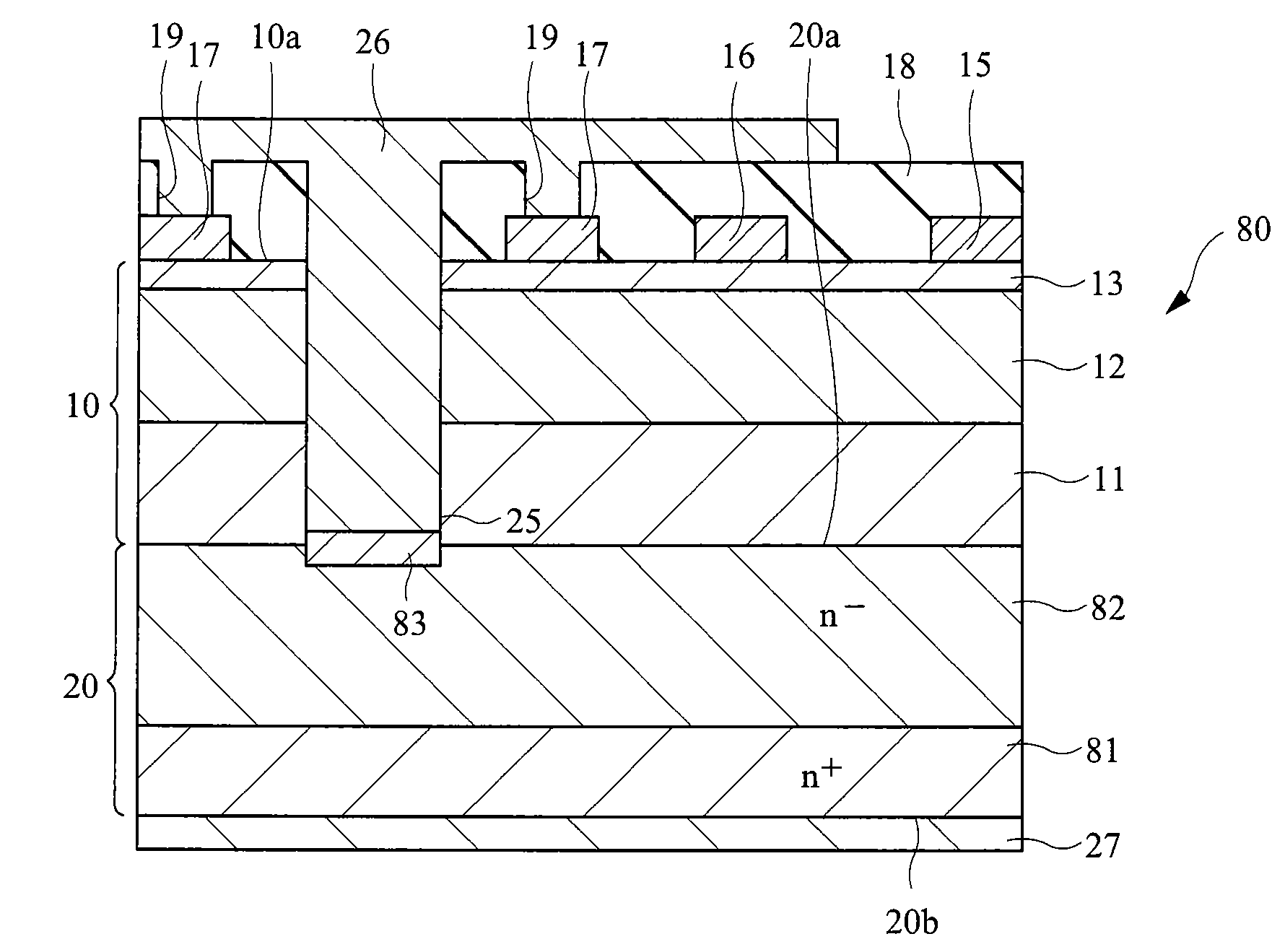
[0098]Next, a semiconductor device of a second embodiment will be described with reference to FIG. 10. FIG. 10 is a cross sectional view showing a main part of a semiconductor chip 40 constituting the semiconductor device of the second embodiment.
[0099]In FIG. 10, the difference between the semiconductor chip 40 of the second embodiment and the semiconductor chip 30 described in the first embodiment lies in that the cathode electrode 27 of the diode is electrically connected to the drain electrode 15 of the transistor in the semiconductor chip 40.
[0100]In the semiconductor chip 40, a via hole (hole) 41 which reaches the n+ layer 21 of the semiconductor substrate 20 from the main surface 10a of the compound semiconductor layer 10 is formed. The via hole 41 penetrates also through the insulating layer 18. In other words, at the stage when the via hole 41 is formed, the upper surface of the n+ layer 21 is exposed on the bottom surface of the via hole 41.
[0101]In addition, a contact hol...
third embodiment
[0112]Next, a semiconductor device of a third embodiment will be described with reference to FIG. 11. FIG. 11 is a cross sectional view showing a main part of a semiconductor chip 50 constituting the semiconductor device of the third embodiment.
[0113]In FIG. 11, the difference between the semiconductor chip 50 of the third embodiment and the semiconductor chip 40 of the second embodiment lies in the electrical connection structure between the cathode electrode 27 and the drain electrode 15.
[0114]More specifically, in the semiconductor chip 50 of the third embodiment, first, an n+ region (third semiconductor region) 51 which extends from the main surface 20a of the semiconductor substrate 20 to the contact surface between the n− layer 22 and the n+ layer 21 is formed in a part of the n− layer 22. Moreover, secondly, the via hole 41 is not formed to the depth where it reaches the n+ layer 21, but is formed to the depth where it reaches the n+ region (third semiconductor region) 51 fro...
PUM
 Abstract
Description
Claims
Application Information