Hybrid monolithic integration

a monolithic integration and hybrid technology, applied in the field of semiconductor structure, can solve the problems of limiting circuit integration to much lower levels, lack of established processes, and relatively limited device speed, and achieves the effects of improving device performance, minimizing cross-contamination possibility, and high density

Active Publication Date: 2012-12-06
QUALCOMM INC
View PDF1 Cites 70 Cited by
  • Summary
  • Abstract
  • Description
  • Claims
  • Application Information

AI Technical Summary

Benefits of technology

[0025]The present invention describes a hybrid integrated circuit comprising both Silicon CMOS and III-V devices, monolithically integrated in a single chip. It allows the almost complete elimination of the contamination issues related to the integration of the different technologies, maintaining at the same time a good planarization of the structure. It further simplify the fabrication process, allowing the growth of high quality III-V materials on (100) silicon substrates lowering the manufacturing cost. Moreover, differently from many prior art attempts, it does not require silicon on insulator technologies and / or other expensive process steps.

Problems solved by technology

While Si technology is more mature and uses more established processes that enable a much higher level of integration, its device speed is relatively limited.
However, III-V compounds semiconductors suffer from extreme sensitivity to processing and a lack of established processes, limiting the circuit integration to much lower levels than for Si IC's.
Nevertheless, the growth of device-quality III-V based hetero-structures on silicon substrates is of huge interest in terms of cost, availability, processing and integration.
Generally however, a mixture of cubic and hexagonal GaN tends to grow on Si (100) substrate, with the cubic poly-type being the dominant phase, which significantly decreases the device performance.
The main difficulty in growing GaN on Si is the stress that develops during growth.
While the basic setup is simple relative to many other deposition techniques, the physical phenomena of laser-target interaction and film growth are quite complex.
Despite these many studies, the high risk of cross-contamination and the defect density limit the manufacture of hybrid integrated circuits.
There are indeed many issues associated with the thermal budget of the combined processes and with the quality of the III-V epitaxial layers, which has not been solved yet.
Even if this method enables the co-integration of two different technologies, it has the disadvantage that the bonding process is still delicate, and may not result in a strong bond.
These grooves are particularly needed at the center of the wafer, where otherwise the bond would not be good enough.
This however implies that the pitches will be present within the final chip, and thus the amount of available surface area decreases.
Even if this solution has the advantage that the integrated semiconductor substrate structure may be provided with a substantially planarized surface, it still does not solve the problem related to the different thermal budgets needed for the III-V process and the CMOS devices.
The high temperature annealing steps required from the CMOS process could lead to the diffusion of Silicon atoms in the GaN layer, decreasing the GaN-based device performances.
The prior art attempts described above have therefore several drawbacks and are not industrially viable.

Method used


Image

  • Hybrid monolithic integration
  • Hybrid monolithic integration
  • Hybrid monolithic integration

Examples


Embodiment Construction
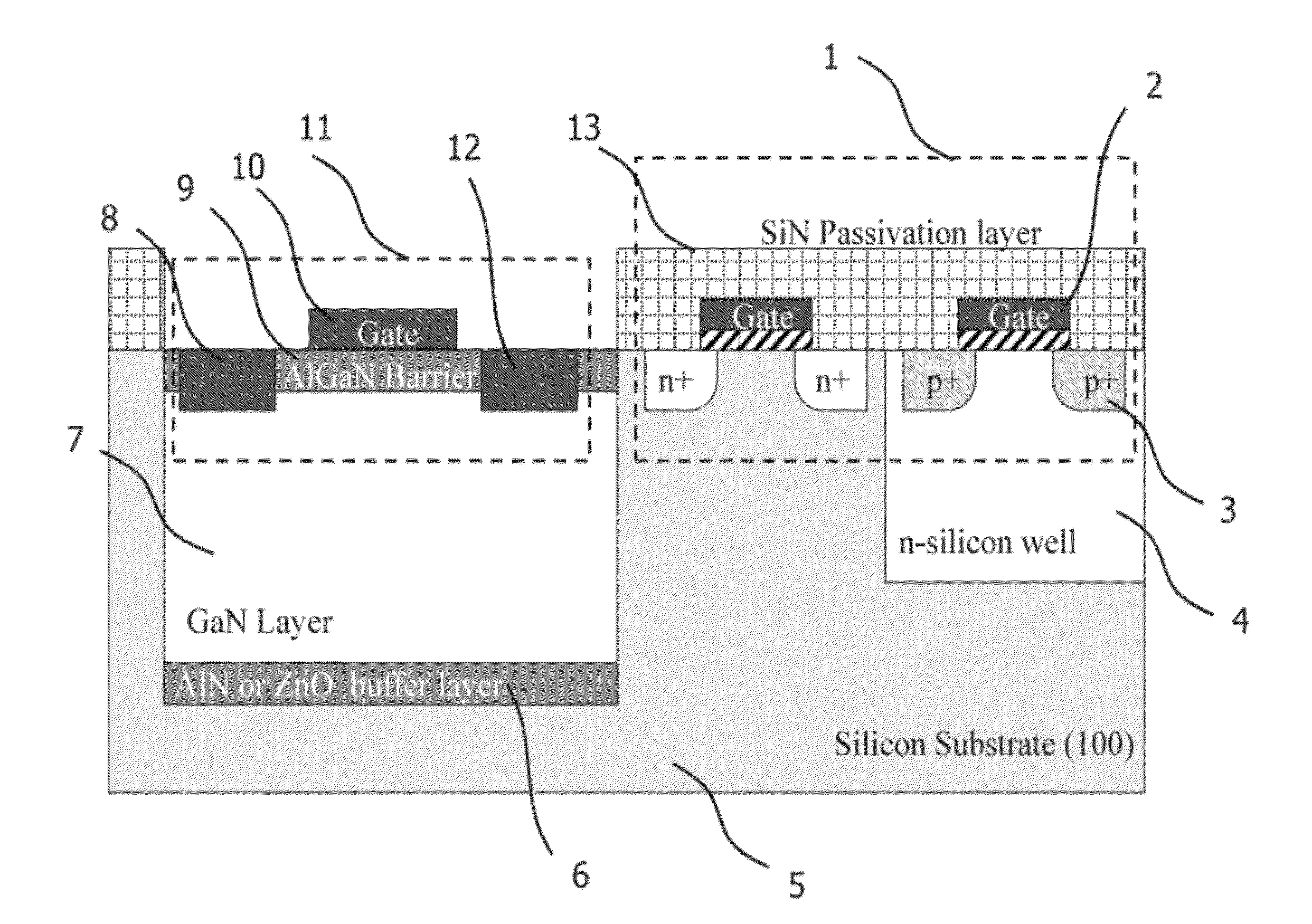
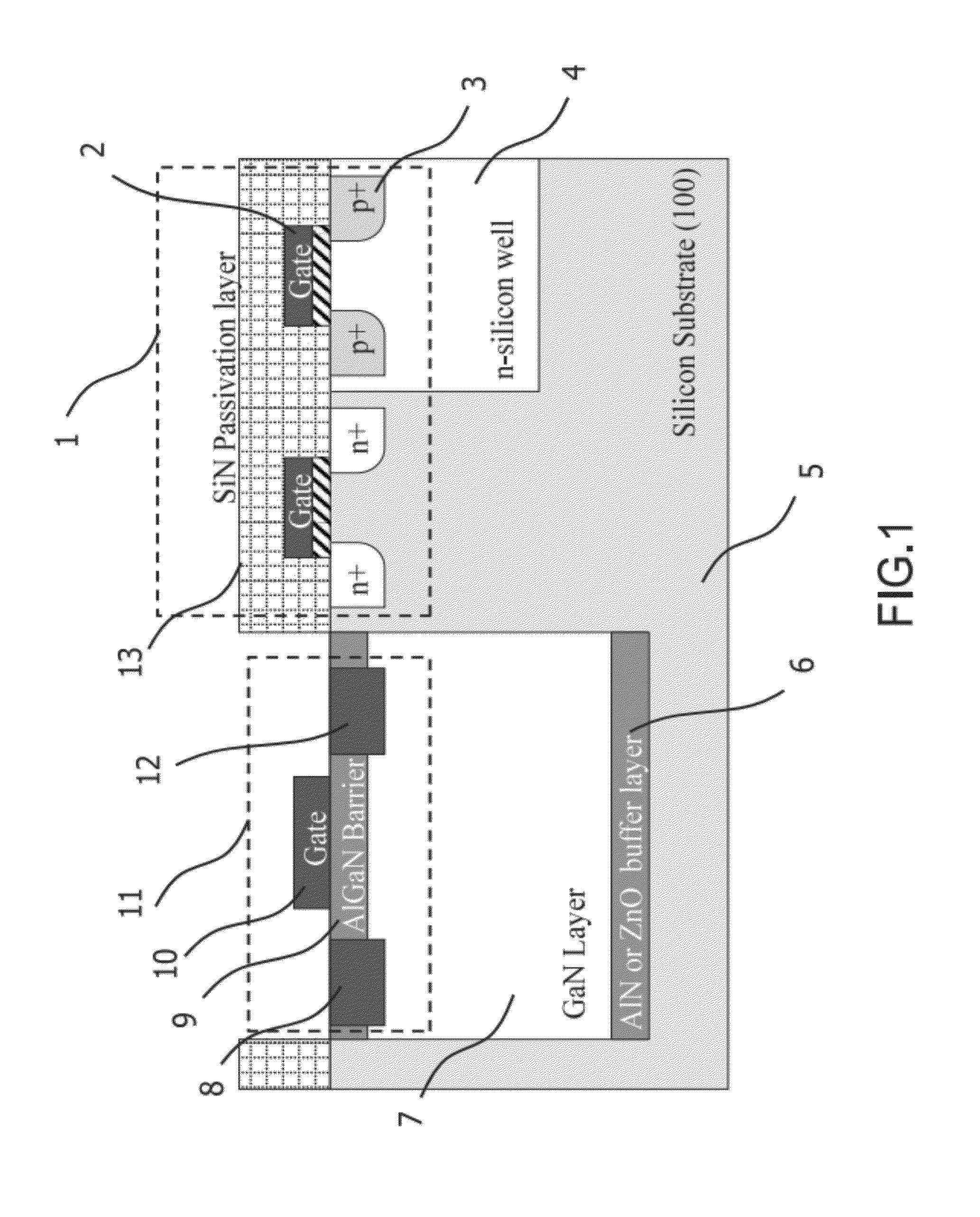
A FIG. 1

[0047]FIG. 1 is showing a cross section view of a hybrid integrated circuit according to a first embodiment of the invention. In this example a CMOS circuit 1 constituted by a re-channel and a p-channel MOSFET, has been co-integrated with a GaN HEMT device 11. The fabrication process of this embodiment includes the following steps: 1) the CMOS circuitry is manufactured in a first Silicon area until the metallization process step; 2) a passivation layer is grown all over the wafer; 3) a trench is formed in a second semiconductor area, using a selective etch; 3) An AlN or ZnO nucleation or buffer layer is formed on the bottom of the silicon trench; 4) A GaN layer is grown through one or more low temperature growth process steps on the top of the nucleation layer.

[0048]Once the GaN layer has been grown, one or more devices can be formed in the III-V region using one or more of the several well known GaN device structures such as enhancement or depletion HEMTs in single, multich...


PUM


Abstract

The present invention describes a hybrid integrated circuit comprising both CMOS and III-V devices, monolithically integrated in a single chip. It allows the almost complete elimination of the contamination issues related to the integration of different technologies, maintaining at the same time a good planarization of the structure. It further simplifies the fabrication process, allowing the growth of high quality III-V materials on (100) silicon substrates lowering the manufacturing cost. Moreover, differently from many prior art attempts, it does not require silicon on insulator technologies and / or other expensive process steps. This invention enables the consolidation on the same integrated circuit of a hybrid switching power converter that takes advantage of the established circuit topologies of CMOS circuitries and of the higher mobility and voltage withstanding of III-V HEMT devices.

Description

RELATED APPLICATION DATA[0001]The present application claims priority from U.S. Provisional Patent Application No. 61 / 520,041 for “Hybrid monolithic integration” filed on Jun. 6, 2011.BACKGROUND OF THE INVENTION[0002]1. Field of the Invention[0003]The present invention is in the field of semiconductor structures. The present invention is further in the field of semiconductor structures of transistor devices and manufacture processes. The present invention further relates to the field of integrated devices and circuits. The implementation is not limited to a specific technology, and applies to either the invention as an individual component or to inclusion of the present invention within larger systems which may be combined into larger integrated circuits.[0004]2. Brief Description of Related Art[0005]Silicon and III-V materials IC technologies are traditionally distinguished by their unique and often exclusive characteristics. While Si technology is more mature and uses more establi...

Claims


Application Information

Patent Timeline
Patent Type & Authority Applications(United States)
IPC IPC(8): H01L29/12H01L21/20
CPCH01L21/02381H01L21/0243H01L21/0245H01L21/02458H01L21/02472H01L21/02494H01L29/2003H01L21/02546H01L21/8258H01L29/7787H01L29/78H01L27/0605H01L27/092H01L21/0254
Inventor MARINO, FABIO ALESSIOMENEGOLI, PAOLO
Owner QUALCOMM INC
Why Eureka
Try Eureka