Probe card and method for manufacturing probe card

a technology of probe card and cantilever, which is applied in the field of probe card, can solve the problems that the cantilever probe needle cannot cope with the testing of the cantilever probe needle cannot be attached at micro intervals on the substrate, and the cantilever probe needle cannot be used to test highly densified and miniaturized wafers. it is easy to flatten, easy to form, and high precision

Inactive Publication Date: 2005-10-13
ADVANTEST CORP
View PDF18 Cites 20 Cited by
  • Summary
  • Abstract
  • Description
  • Claims
  • Application Information

AI Technical Summary

Benefits of technology

[0033] Furthermore, according to the probe card of the present invention, as described in claim 6, the flat portion can be constituted of a mask layer formed on the substrate. Thus, in the present invention, the flat portion can be formed by the mask layer constituted, for example, of a metal mask, a mesh mask or the like. Moreover, the surface of the mask layer is polished or processed otherwise, and can be easily flattened. Accordingly, the flat portion according to the present invention can be easily formed with high precision. Especially when the flat portion is constituted of the mask layer, the flat portion can be formed broadly in a plane form on the surface of the substrate, and the mounting of the probe needle can be facilitated.
[0034] Additionally, in the probe card of the present invention, as described in claim 7, the flat portion can be constituted of a built-up layer formed on the substrate. Therefore, in the present invention, when the built-up layer (built-up portion) is disposed on the surface of the substrate, the built-up layer is polished, and accordingly the flat portion according to the present invention can be formed directly on the built-up layer. When the built-up layer is directly polished to form the flat portion, the flat portion according to the present invention can be formed broadly in a plane manner on the surface of the substrate in the same manner as in a case where the flat portion is constituted of the mask layer. When the flat portion is formed directly on the built-up layer in this manner, the flat portion according to the present invention can be formed more easily and efficiently, and the whole probe card can be thinned and lightened.
[0035] Moreover, in the probe card of the present invention, as described in claim 8, the probe needle is formed separately from the substrate, and can be constituted to be mounted on the flat portion. Especially, as described in claim 9, the probe needle can be constituted to include a base portion and a plurality of needle portions protruding from the base portion in a comb shape. As described in claim 10, the probe needle may be constituted of silicon formed into a needle shape, and a conductive pattern formed on the surface of silicon. Therefore, according to the present invention, when silicon is etched, the probe needles which are separate from the substrate can be formed to be fine with high precision. Accordingly, the fine probe needles suitable for the probe card of the present invention including the flat portion can be easily formed with high precision. Since the probe needle is formed in a comb shape (finger shape) including a large number of fine needles, a large number of probe needles can be mounted on the substrate by one operation, an operation for mounting the probe needles can be remarkably easily performed, and the probe card according to the present invention can be easily and efficiently manufactured. It is to be noted that the probe needles formed of silicon or the like separately from the substrate can be, needless to say, formed into individual needles. Even in this case, needless to say, the needles are applicable to the probe card including the flat portion of the present invention.
[0036] On the other hand, in the probe card of the present invention, as described in claim 11, the probe needle can be formed directly on the surface of the flat portion. Moreover, as described in claim 12, the probe needle can be plated / formed into a needle shape on the surface of the flat portion. Therefore, according to the present invention, the high-precision fine probe needle can be formed directly on the flat portion, for example, by nickel plating or the like. As the probe needle by the plating, the fine plated needle can be easily formed with high precision, when masking and plating are repeated a plurality of times on the flat portion. Accordingly, the fine probe needle suitable for the probe card of the present invention including the flat portion can be easily formed with high precision. When the probe needle is formed directly on the flat portion by the plating in this manner, a need for an operation for mounting the needle onto the substrate or connecting the needle to the wiring pattern can be obviated, and the probe card according to the present invention can be easily and efficiently manufactured.
[0037] Moreover, according to the present invention, as described in claim 13, there is a method of manufacturing a probe card, in which the surface for mounting a probe needle is flattened to form a flat portion on the surface of a substrate of the probe card including: the substrate having a wiring pattern for transmitting a test signal to be applied to a wafer constituting a testing object; and a probe needle disposed on the substrate and connected to the wiring pattern to contact an electrode of the wafer, the method comprising: a step of forming a mask on the substrate on which a predetermined wiring pattern is formed; a step of forming an opening at a predetermined position of the mask; a step of plating the opening; and a step of polishing and flattening the surface of the mask. As described in claim 14, the method further comprises: a step of peeling the mask after the step of polishing and flattening the surface of the mask. Therefore, according to the present invention, the flat portion according to the present invention can be easily formed on the wiring pattern of the substrate or in another desired position with high precision by masking, patterning, plating and the like. Moreover, the surface of the flat portion can be formed into a plane using the lap polishing and the like, so that the probe card according to the present invention can be easily manufactured. It is to be noted that another method or step may also be used as long as unevenness, difference of elevation or the like of the surface of the substrate is corrected and the flat portion having high flatness can be formed.
[0038] Furthermore, according to the present invention, as described in claim 15, there is provided a method of manufacturing a probe card, in which the surface for mounting a probe needle is flattened to form a flat portion on the surface of a substrate of the probe card including: the substrate having a wiring pattern for transmitting a test signal to be applied to a wafer constituting a testing object; and a probe needle disposed on the substrate and connected to the wiring pattern to contact an electrode of the wafer, the method comprising: a step of forming a built-up portion on the substrate on which a predetermined wiring pattern is formed; and a step of polishing and flattening the surface of the built-up portion. Therefore, according to the present invention, since the built-up portion (built-up layer) is formed on the surface of the substrate, and the built-up portion is polished, the flat portion obtained by forming the surface into the plane with high precision can be formed directly on the built-up layer. When the flat portion is formed directly on the built-up portion in this manner, it is possible to more easily and efficiently manufacture the probe card including the flat portion.

Problems solved by technology

However, a problem has occurred that the conventional probe card including the cantilevered probe needles cannot cope with the testing of highly densified and miniaturized wafers in recent years.
In the conventional probe card, the cantilevered probe needle itself has a diameter of about 250 μm, all the probe needles have been attached by the manual operation, and therefore it has been impossible to attach a large probe needles at micro intervals on the substrate.
Therefore, in recent years, the highly densified and miniaturized wafers have not been tested with the cantilevered probe card.
Additionally, in the cantilevered probe needle, there has been a problem that high frequency characteristics are deteriorated because the total length of the needle is about 30 to 50 mm.
However, the membrane type probe card has required a large number of complicated constituting elements such as a membrane including the electrode bumps, a holding structure which holds the membrane, and pressurizing means for energizing the membrane toward a wafer side.
Therefore, the probe card and wafer tester have been complicated and enlarged, and manufacturing costs have also increased as compared with the conventional cantilevered type.
However, thereafter it has been realized that even when the fine probe needles can be formed with high precision, and when the fine probe needles are simply mounted on the substrate, the needle heights of the probe needles are not uniform by unevenness of the substrate.
Additionally, the fluctuations cannot be absorbed within the elasticity limit by the probe needles having micro needle tips unlike the conventional cantilevered needle.

Method used


Image

  • Probe card and method for manufacturing probe card
  • Probe card and method for manufacturing probe card
  • Probe card and method for manufacturing probe card

Examples


first embodiment

[0053] First, a first embodiment of the probe card according to the present invention will be described with reference to FIGS. 1 to 9.

[Wafer Tester]

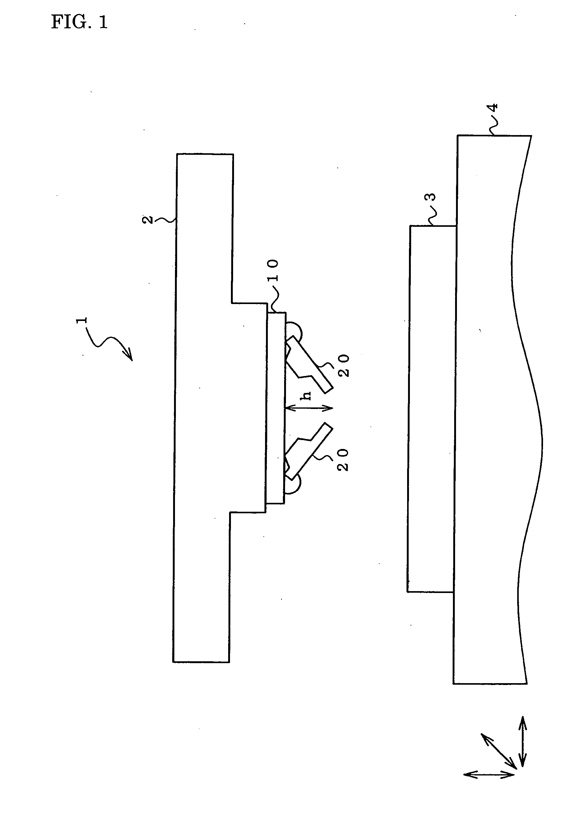
[0054]FIG. 1 is a front view schematically showing a wafer tester including a probe card according to a first embodiment of the present invention.

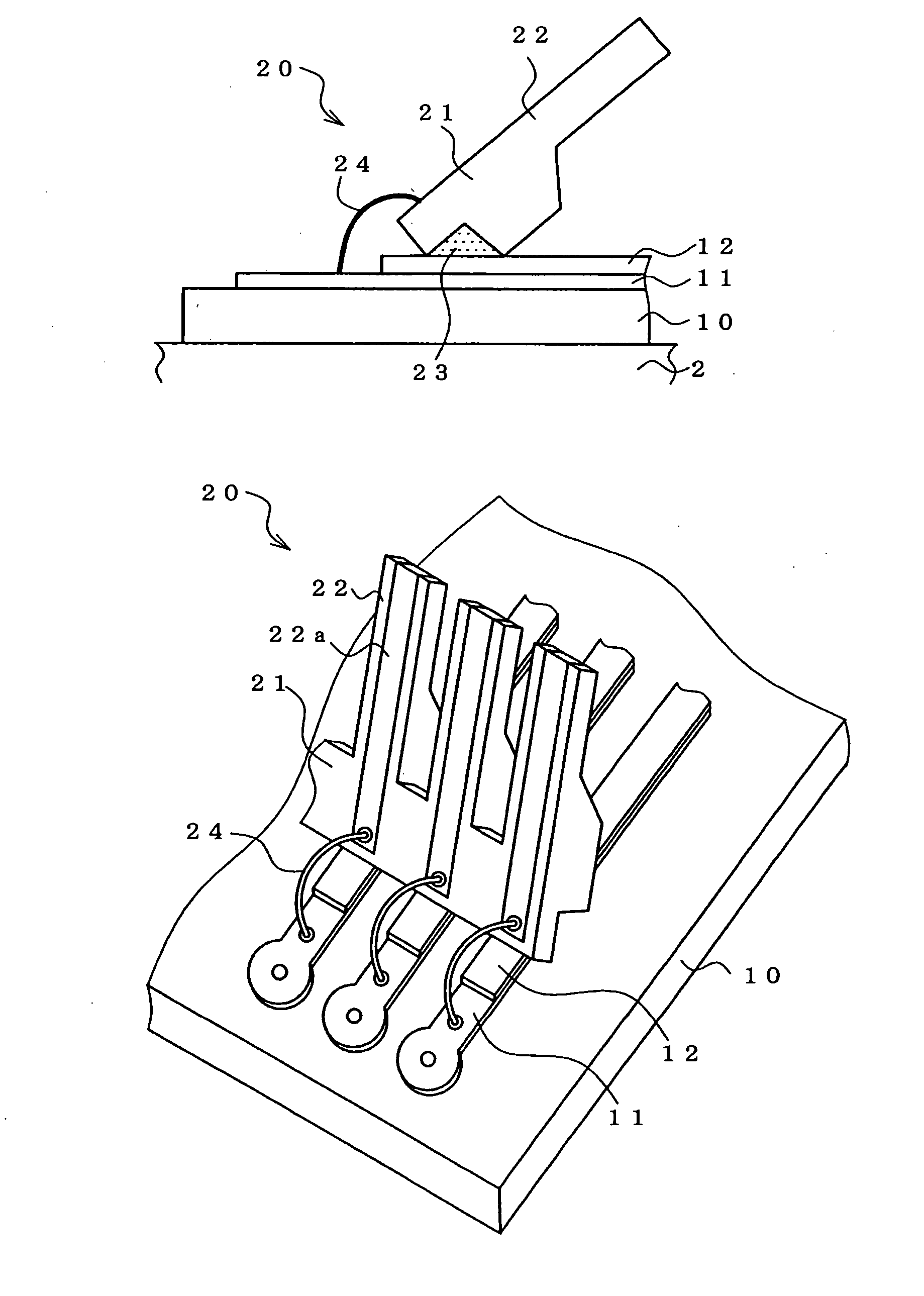
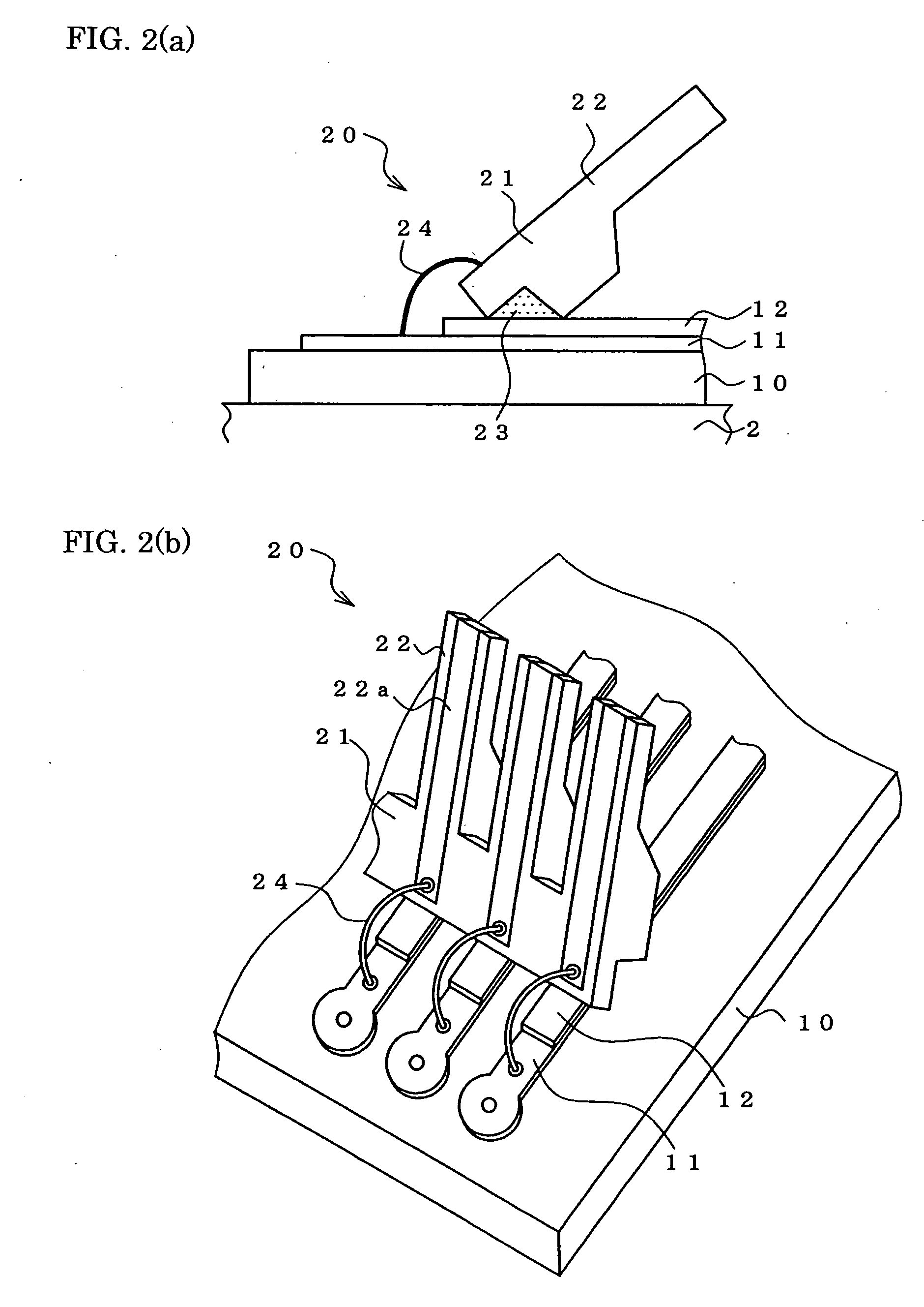
[0055] The wafer tester is a device for testing electric properties of each device in a state of a wafer before a plurality of semiconductor device chips formed on the wafer (semiconductor substrate) are cut into individual chips and sealed into a package, a so-called semi-finished product state, and is also called a wafer prober. Concretely, as shown in FIG. 1, the wafer tester includes a wafer base 4 on which a wafer 3 constituting a testing object is mounted, and a probe card 1 positioned above the wafer base 4 according to the present embodiment.

[0056] The probe card 1 includes a plurality of probe needles 20 on a board 2 constituted of a printed board or the like which transmits a pre...

second embodiment

[Second Embodiment]

[0102] Next, a second embodiment of a probe card according to the present invention will be described with reference to FIGS. 11 and 12.

[0103]FIG. 11 schematically shows a state in which the probe card according to the second embodiment of the present invention is vertically reversed, (a) is a main part enlarged front view, and (b) is a perspective view.

[0104]FIG. 12 schematically shows a probe needle formed on the probe card according to the present embodiment, (a) is a plan view, (b) is a front view, and (c) is a left side view.

[0105] As shown in these figures, the probe card according to the present embodiment is a modified embodiment of the above-described first embodiment, and as the probe needle mounted on the flat portion, a nickel-plated probe needle is used instead of the silicon-formed probe needle formed into the comb shape in the first embodiment. Therefore, other constituting portions are similar to those of the first embodiment, and the similar co...


PUM

PropertyMeasurementUnit
total lengthaaaaaaaaaa
sizeaaaaaaaaaa

Abstract

A probe card on which micro probe needles are arranged at high density and with high precision with neither the need of a complicated structure or variation in needle height. A probe card 1 installed in a wafer tester comprises a board 2 having a wiring pattern for transmitting a test signal to be impressed on a wafer under test, a built-up board 10 formed on the surface of the board 2, a comb-shaped silicon-made probe needle 20 arranged on the built-up board 10 and connected to the surface wiring pattern 11, and a flat portion 12 formed by plating on the surface wiring pattern 11 on the built-up board 10 and having a surface flattened by polishing. The probe needle 20 is loaded on the flat portion 12 and thus mounted on the board 2.

Description

TECHNICAL FIELD [0001] The present invention relates to a probe card disposed in a wafer tester (wafer prober) for performing an electric property test of a wafer which is not packaged. [0002] Particularly, the present invention relates to a probe card and a method of manufacturing the probe card in which probe needles to contact electrodes of a wafer are formed to be fine using silicon, nickel and the like and in which a flat portion is flattened with high precision and formed on a substrate including the probe needles mounted / fixed thereon and in which micro probe needles can be arranged disposed at high density and with precision without requiring any complicated structure or the like or without any variation in needle height. BACKGROUND ART [0003] In general, a plurality of semiconductor device chips formed on a wafer (semiconductor substrate) are tested for electric properties of each device and the like in a state of a wafer before cut into individual chips and sealed into pac...

Claims


Application Information

Patent Timeline
Patent Type & Authority Applications(United States)
IPC IPC(8): G01R1/073
CPCG01R1/07307G01R1/07342Y10T29/49165Y10T29/49155H01L22/00
Inventor KOJIMA, AKIO
Owner ADVANTEST CORP
Why Eureka
Try Eureka